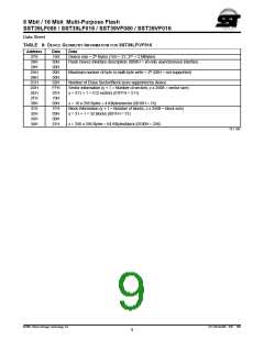
8 Mbit / 16 Mbit Multi-Purpose Flash
SST39LF080 / SST39LF016 / SST39VF080 / SST39VF016
Data Sheet
are Data# Polling and Toggle Bit. During the internal Pro-
gram operation, the host is free to perform additional tasks.
Any commands issued during the internal Program opera-
tion are ignored.
Device Operation
Commands are used to initiate the memory operation func-
tions of the device. Commands are written to the device
using standard microprocessor write sequences. A com-
mand is written by asserting WE# low while keeping CE#
low. The address bus is latched on the falling edge of WE#
or CE#, whichever occurs last. The data bus is latched on
the rising edge of WE# or CE#, whichever occurs first.
Sector/Block-Erase Operation
The Sector- (or Block-) Erase operation allows the system
to erase the device on a sector-by-sector (or block-by-
block) basis. The SST39LF/VF080 and SST39LF/VF016
offer both Sector-Erase and Block-Erase mode. The sector
architecture is based on uniform sector size of 4 KByte.
The Block-Erase mode is based on uniform block size of
64 KByte. The Sector-Erase operation is initiated by exe-
cuting a six-byte-command sequence with Sector-Erase
command (30H) and sector address (SA) in the last bus
cycle. The Block-Erase operation is initiated by executing a
six-byte-command sequence with Block-Erase command
(50H) and block address (BA) in the last bus cycle. The
sector or block address is latched on the falling edge of the
sixth WE# pulse, while the command (30H or 50H) is
latched on the rising edge of the sixth WE# pulse. The
internal Erase operation begins after the sixth WE# pulse.
The End-of-Erase operation can be determined using
either Data# Polling or Toggle Bit methods. See Figures 9
and 10 for timing waveforms. Any commands issued during
the Sector- or Block-Erase operation are ignored.
The SST39LF/VF080 and SST39LF/VF016 also have the
Auto Low Power mode which puts the device in a near
standby mode after data has been accessed with a valid
Read operation. This reduces the IDD active read current
from typically 15 mA to typically 4 µA. The Auto Low Power
mode reduces the typical IDD active read current to the
range of 1 mA/MHz of read cycle time. The device exits the
Auto Low Power mode with any address transition or con-
trol signal transition used to initiate another Read cycle,
with no access time penalty. Note that the device does not
enter Auto Low Power mode after power-up with CE# held
steadily low until the first address transition or CE# is driven
high.
Read
The Read operation of the SST39LF/VF080 and
SST39LF/VF016 is controlled by CE# and OE#, both have
to be low for the system to obtain data from the outputs.
CE# is used for device selection. When CE# is high, the
chip is deselected and only standby power is consumed.
OE# is the output control and is used to gate data from the
output pins. The data bus is in high impedance state when
either CE# or OE# is high. Refer to the Read cycle timing
diagram for further details (Figure 3).
Chip-Erase Operation
The SST39LF/VF080 and SST39LF/VF016 provide a
Chip-Erase operation, which allows the user to erase the
entire memory array to the “1” state. This is useful when the
entire device must be quickly erased.
The Chip-Erase operation is initiated by executing a six
byte command sequence with Chip-Erase command (10H)
at address 5555H in the last byte sequence. The Erase
operation begins with the rising edge of the sixth WE# or
CE#, whichever occurs first. During the Erase operation,
the only valid read is Toggle Bit or Data# Polling. See Table
4 for the command sequence, Figure 8 for timing diagram,
and Figure 19 for the flowchart. Any commands issued dur-
ing the Chip-Erase operation are ignored.
Byte-Program Operation
The SST39LF/VF080 and SST39LF/VF016 are pro-
grammed on a byte-by-byte basis. Before programming,
one must ensure that the sector, in which the byte which is
being programmed exists, is fully erased. The Program
operation consists of three steps. The first step is the three-
byte load sequence for Software Data Protection. The sec-
ond step is to load byte address and byte data. During the
Byte-Program operation, the addresses are latched on the
falling edge of either CE# or WE#, whichever occurs last.
The data is latched on the rising edge of either CE# or
WE#, whichever occurs first. The third step is the internal
Program operation which is initiated after the rising edge of
the fourth WE# or CE#, whichever occurs first. The Pro-
gram operation, once initiated, will be completed within 20
µs. See Figures 4 and 5 for WE# and CE# controlled Pro-
gram operation timing diagrams and Figure 16 for flow-
charts. During the Program operation, the only valid reads
Write Operation Status Detection
The SST39LF/VF080 and SST39LF/VF016 provide two
software means to detect the completion of a write (Pro-
gram or Erase) cycle, in order to optimize the system Write
cycle time. The software detection includes two status bits:
Data# Polling (DQ7) and Toggle Bit (DQ6). The End-of-Write
detection mode is enabled after the rising edge of WE#,
which initiates the internal Program or Erase operation.
©2001 Silicon Storage Technology, Inc.
S71146-03-000 6/01 396
2

 SST [ SILICON STORAGE TECHNOLOGY, INC ]