8 Mbit / 16 Mbit Multi-Purpose Flash
SST39LF080 / SST39LF016 / SST39VF080 / SST39VF016
Data Sheet
The actual completion of the nonvolatile write is asynchro-
Hardware Data Protection
nous with the system; therefore, either a Data# Polling or
Toggle Bit read may be simultaneous with the completion
of the Write cycle. If this occurs, the system may possibly
get an erroneous result, i.e., valid data may appear to con-
flict with either DQ7 or DQ6. In order to prevent spurious
rejection, if an erroneous result occurs, the software routine
should include a loop to read the accessed location an
additional two (2) times. If both reads are valid, then the
device has completed the Write cycle, otherwise the rejec-
tion is valid.
Noise/Glitch Protection: A WE# or CE# pulse of less than 5
ns will not initiate a Write cycle.
VDD Power Up/Down Detection: The Write operation is
inhibited when VDD is less than 1.5V.
Write Inhibit Mode: Forcing OE# low, CE# high, or WE#
high will inhibit the Write operation. This prevents inadvert-
ent writes during power-up or power-down.
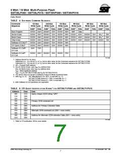
Software Data Protection (SDP)
The SST39LF/VF080 and SST39LF/VF016 provide the
JEDEC approved Software Data Protection scheme for all
data alteration operations, i.e., Program and Erase. Any
Program operation requires the inclusion of the three-byte
sequence. The three-byte load sequence is used to initiate
the Program operation, providing optimal protection from
inadvertent Write operations, e.g., during the system
power-up or power-down. Any Erase operation requires the
inclusion of six-byte sequence. The SST39LF/VF080 and
SST39LF/VF016 devices are shipped with the Software
Data Protection permanently enabled. See Table 4 for the
specific software command codes. During SDP command
sequence, invalid commands will abort the device to read
Data# Polling (DQ7)
When the SST39LF/VF080 and SST39LF/VF016 are in
the internal Program operation, any attempt to read DQ7
will produce the complement of the true data. Once the
Program operation is completed, DQ7 will produce true
data. The device is then ready for the next operation. Dur-
ing internal Erase operation, any attempt to read DQ7 will
produce a ‘0’. Once the internal Erase operation is com-
pleted, DQ7 will produce a ‘1’. The Data# Polling is valid
after the rising edge of fourth WE# (or CE#) pulse for Pro-
gram operation. For Sector-, Block- or Chip-Erase, the
Data# Polling is valid after the rising edge of sixth WE# (or
CE#) pulse. See Figure 6 for Data# Polling timing diagram
and Figure 17 for a flowchart.
mode within TRC
.
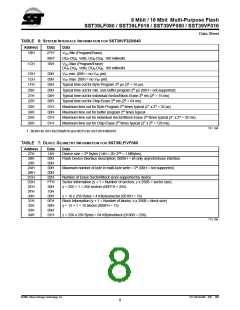
Common Flash Memory Interface (CFI)
Toggle Bit (DQ6)
The SST39LF/VF080 and SST39LF/VF016 also contain
the CFI information to describe the characteristics of the
device. In order to enter the CFI Query mode, the system
must write three-byte sequence, same as product ID entry
command with 98H (CFI Query command) to address
5555H in the last byte sequence. Once the device enters
the CFI Query mode, the system can read CFI data at the
addresses given in Tables 5 through 8. The system must
write the CFI Exit command to return to Read mode from
the CFI Query mode.
During the internal Program or Erase operation, any con-
secutive attempts to read DQ6 will produce alternating 1s
and 0s, i.e., toggling between 1 and 0. When the internal
Program or Erase operation is completed, the DQ6 bit will
stop toggling. The device is then ready for the next opera-
tion. The Toggle Bit is valid after the rising edge of fourth
WE# (or CE#) pulse for Program operation. For Sector-,
Block-, or Chip-Erase, the Toggle Bit is valid after the rising
edge of sixth WE# (or CE#) pulse. See Figure 7 for Toggle
Bit timing diagram and Figure 17 for a flowchart.
Data Protection
The SST39LF/VF080 and SST39LF/VF016 provide both
hardware and software features to protect nonvolatile data
from inadvertent writes.
©2001 Silicon Storage Technology, Inc.
S71146-03-000 6/01 396
3

 SST [ SILICON STORAGE TECHNOLOGY, INC ]