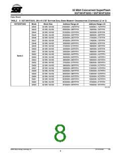
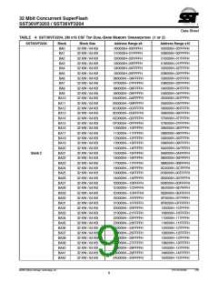
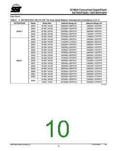
32 Mbit Concurrent SuperFlash
SST36VF3203 / SST36VF3204
Data Sheet
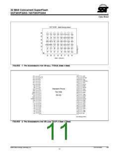
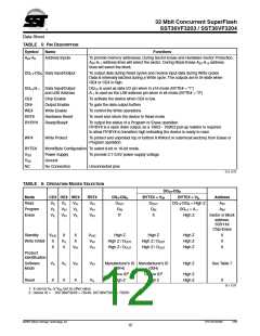
TABLE 5: PIN DESCRIPTION
Symbol
Name
Functions
A20-A0
Address Inputs
To provide memory addresses. During Sector-Erase and Hardware Sector Protection,
A20-A11 address lines will select the sector. During Block-Erase A20-A15 address
lines will select the block.
DQ14-DQ0 Data Input/Output
To output data during Read cycles and receive input data during Write cycles
Data is internally latched during a Write cycle. The outputs are in tri-state when
OE# or CE# is high.
DQ15/A-1 Data Input/Output
and LBS Address
DQ15 is used as data I/O pin when in x16 mode (BYTE# = “1”)
A-1 is used as the LSB address pin when in x8 mode (BYTE# = “0”)
CE#
Chip Enable
To activate the device when CE# is low.
To gate the data output buffers
OE#
Output Enable
Write Enable
Hardware Reset
Ready/Busy#
WE#
To control the Write operations
RST#
RY/BY#
To reset and return the device to Read mode
To output the status of a Program or Erase operation
RY/BY# is a open drain output, so a 10KΩ - 100KΩ pull-up resistor is required
to allow RY/BY# to transition high indicating the device is ready to read.
WP#
Write Protect
To protect and unprotect top or bottom 8 KWord (4 outermost sectors) from Erase or
Program operation.
BYTE#
VDD
Word/Byte Configuration To select 8-bit or 16-bit mode.
Power Supply
Ground
To provide 2.7-3.6V power supply voltage
VSS
NC
No Connection
Unconnected pins
T5.0 1270
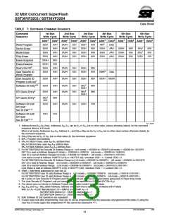
TABLE 6: OPERATION MODES SELECTION
DQ15-DQ8
Mode
Read
CE# OE# WE#
RST#
VIH
DQ7-DQ0
DOUT
DIN
BYTE# = VIH
BYTE# = VIL
DQ14-DQ8 = High Z
DQ15 = A-1
Address
VIL
VIL
VIL
VIL
VIH
VIH
VIH
VIL
VIL
DOUT
DIN
X
AIN
AIN
Program
Erase
VIH
VIH
X1
High Z
Sector or Block
address,
555H for
Chip-Erase
Standby
VIHC
X
X
VIL
X
X
X
VIHC
VIH
High Z
High Z
High Z
High Z
High Z
X
X
X
Write Inhibit
High Z / DOUT
High Z / DOUT
High Z / DOUT
High Z / DOUT
X
VIH
VIH
Product
Identification
Software
Mode
VIL
X
VIL
X
VIH
VIH
Manufacturer’s ID Manufacturer’s ID
High Z
See Table 7
(BFH)
Device ID2
High Z
(00H)
Device ID2
High Z
High Z
High Z
Reset
X
VIL
X
T6.1 1270
1. X can be VIL or VIH, but no other value.
2. Device ID = SST36VF3203 = 7354H, SST36VF3204 = 7353H
©2005 Silicon Storage Technology, Inc.
S71270-03-000
7/06
12

 SST [ SILICON STORAGE TECHNOLOGY, INC ]