32 Mbit (x8/x16) Concurrent SuperFlash
SST36VF3203 / SST36VF3204
SST36VF3201C / 1602C32Mb (x8/x16) Concurrent SuperFlash
Data Sheet
FEATURES:
•
•
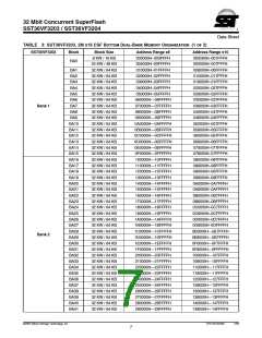
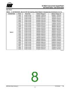
Organized as 2M x16 or 4M x8
Dual Bank Architecture for Concurrent
Read/Write Operation
– 32 Mbit Bottom Sector Protection
(in the smaller bank)
- SST36VF3203: 8 Mbit + 24 Mbit
– 32 Mbit Top Sector Protection
(in the smaller bank)
•
Block-Erase Capability
– Uniform 32 KWord blocks
Erase-Suspend / Erase-Resume Capabilities
Security ID Feature
– SST: 128 bits
•
•
– User: 256 Bytes
•
Fast Read Access Time
– 70 ns
- SST36VF3204: 24 Mbit + 8 Mbit
•
•
Single 2.7-3.6V for Read and Write Operations
Superior Reliability
•
•
Latched Address and Data
Fast Erase and Program (typical):
– Endurance: 100,000 cycles (typical)
– Greater than 100 years Data Retention
Low Power Consumption:
– Active Current: 6 mA typical
– Standby Current: 4 µA typical
– Auto Low Power Mode: 4 µA typical
– Sector-Erase Time: 18 ms
– Block-Erase Time: 18 ms
– Chip-Erase Time: 35 ms
– Program Time: 7 µs
Automatic Write Timing
– Internal VPP Generation
End-of-Write Detection
•
•
•
•
•
Hardware Sector Protection/WP# Input Pin
– Protects 8 KWord in the smaller bank by driving
WP# low and unprotects by driving WP# high
Hardware Reset Pin (RST#)
– Toggle Bit
– Data# Polling
– Ready/Busy# pin
•
•
•
CMOS I/O Compatibility
Conforms to Common Flash Memory Interface (CFI)
JEDEC Standards
– Flash EEPROM Pinouts and command sets
Packages Available
– 48-ball TFBGA (6mm x 8mm)
– 48-lead TSOP (12mm x 20mm)
– Resets the internal state machine to reading
array data
Byte# Pin
– Selects 8-bit or 16-bit mode
Sector-Erase Capability
– Uniform 2 KWord sectors
Chip-Erase Capability
•
•
•
•
•
All non-Pb (lead-free) devices are RoHS compliant
PRODUCT DESCRIPTION
The SST36VF320x are 2M x16 or 4M x8 CMOS Concur-
rent Read/Write Flash Memory manufactured with SST’s
proprietary, high performance CMOS SuperFlash technol-
ogy. The split-gate cell design and thick-oxide tunneling
injector attain better reliability and manufacturability com-
pared with alternate approaches. The devices write (Pro-
gram or Erase) with a 2.7-3.6V power supply and conform
to JEDEC standard pinouts for x8/x16 memories.
and tested for a wide spectrum of applications, these
devices are offered with a guaranteed endurance of 10,000
cycles. Data retention is rated at greater than 100 years.
These devices are suited for applications that require con-
venient and economical updating of program, configura-
tion, or data memory. For all system applications, the
devices significantly improve performance and reliability,
while lowering power consumption. Since for any given
voltage range, the SuperFlash technology uses less cur-
rent to program and has a shorter erase time, the total
energy consumed during any Erase or Program operation
is less than alternative flash technologies. These devices
also improve flexibility while lowering the cost for program,
data, and configuration storage applications.
Featuring high performance Word-Program, these devices
provide a typical Program time of 7 µsec and use the Tog-
gle Bit, Data# Polling, or RY/BY# to detect the completion
of the Program or Erase operation. To protect against inad-
vertent write, the devices have on-chip hardware and Soft-
ware Data Protection schemes. Designed, manufactured,
©2005 Silicon Storage Technology, Inc.
The SST logo and SuperFlash are registered trademarks of Silicon Storage Technology, Inc.
CSF is a trademark of Silicon Storage Technology, Inc.
S71270-03-000
1
7/06
These specifications are subject to change without notice.

 SST [ SILICON STORAGE TECHNOLOGY, INC ]