16 Mbit Concurrent SuperFlash + 2/4/8 Mbit SRAM ComboMemory
SST34HF1602C / SST34HF1622C / SST34HF1642C
SST34HF1642D / SST34HF1682D / SST34HF1622S / SST34HF1642S
Advance Information
Product Identification
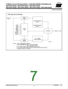
(P)SRAM Operation
The Product Identification mode identifies the device as the
SST34HF16x2C/D/S and manufacturer as SST. This
mode may be accessed by software operations only. The
hardware device ID Read operation, which is typically used
by programmers cannot be used on this device because of
the shared lines between flash and (P)SRAM in the multi-
chip package. Therefore, application of high voltage to pin
A9 may damage this device. Users may use the software
Product Identification operation to identify the part (i.e.,
using the device ID) when using multiple manufacturers in
the same socket. For details, see Tables 4 and 7 for soft-
ware operation, Figure 16 for the Software ID Entry and
Read timing diagram and Figure 24 for the ID Entry com-
mand sequence flowchart.
With BES1# low, BES2 and BEF# high, the
SST34HF16x2C/D/S operate as either 128K x16, 256K
x16, or 512K x16 CMOS (P)SRAM, with fully static opera-
tion requiring no external clocks or timing strobes. The
SST34HF16x2C/D/S (P)SRAM is mapped into the first 512
KWord address space. When BES1#, BEF# are high and
BES2 is low, all memory banks are deselected and the
device enters standby. Read and Write cycle times are
equal. The control signals UBS# and LBS# provide access
to the upper data byte and lower data byte (UBS# and
LBS# signals are NC for SST3416x2S parts). See Table 4
for x16 (P)SRAM Read and Write data byte control modes
of operation. See Table 5 for x8 SRAM Read and Write
data byte control modes of operation.
TABLE 2: PRODUCT IDENTIFICATION
ADDRESS DATA
(P)SRAM Read
The (P)SRAM Read operation of the SST34HF16x2C/D/S
is controlled by OE# and BES1#, both have to be low with
WE# and BES2 high for the system to obtain data from the
outputs. BES1# and BES2 are used for (P)SRAM bank
selection. OE# is the output control and is used to gate
data from the output pins. The data bus is in high imped-
ance state when OE# is high. Refer to the Read cycle tim-
ing diagram, Figure 5, for further details.
Manufacturer’s ID
Device ID
BK0000H
00BFH
SST34HF16x2C/D/S
BK0001H
734AH
T2.0 1256
Note: BK = Bank Address (A19-A18
)
Product Identification Mode Exit
(P)SRAM Write
In order to return to the standard Read mode, the Software
Product Identification mode must be exited. Exit is accom-
plished by issuing the Software ID Exit command
sequence, which returns the device to the Read mode.
This command may also be used to reset the device to the
Read mode after any inadvertent transient condition that
apparently causes the device to behave abnormally, e.g.,
not read correctly. Please note that the Software ID Exit
command is ignored during an internal Program or Erase
operation. See Table 7 for software command codes, Fig-
ure 17 for timing waveform and Figure 24 for a flowchart.
The (P)SRAM Write operation of the SST34HF16x2C/D/S
is controlled by WE# and BES1#, both have to be low,
BES2 must be high for the system to write to the (P)SRAM.
During the Word-Write operation, the addresses and data
are referenced to the rising edge of either BES1#, WE#, or
the falling edge of BES2 whichever occurs first. The write
time is measured from the last falling edge of BES#1 or
WE# or the rising edge of BES2 to the first rising edge of
BES1#, or WE# or the falling edge of BES2. Refer to the
Write cycle timing diagrams, Figures 6 and 7, for further
details.
©2004 Silicon Storage Technology, Inc.
S71256-00-000
3/04
6

 SST [ SILICON STORAGE TECHNOLOGY, INC ]