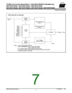
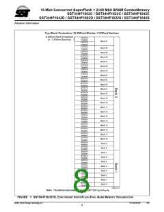
16 Mbit Concurrent SuperFlash + 2/4/8 Mbit SRAM ComboMemory
SST34HF1602C / SST34HF1622C / SST34HF1642C
SST34HF1642D / SST34HF1682D / SST34HF1622S / SST34HF1642S
Advance Information
Flash Word-/Byte-Program Operation
Flash Chip-Erase Operation
These devices are programmed on a word-by-word or
byte-by-byte basis depending on the state of the CIOF pin.
Before programming, one must ensure that the sector
which is being programmed is fully erased.
The SST34HF16x2C/D/S provide a Chip-Erase operation,
which allows the user to erase all sectors/blocks to the “1”
state. This is useful when the device must be quickly
erased.
The Program operation is accomplished in three steps:
The Chip-Erase operation is initiated by executing a six-
byte command sequence with Chip-Erase command (10H)
at address 5555H in the last byte sequence. The Erase
operation begins with the rising edge of the sixth WE# or
BEF#, whichever occurs first. During the Erase operation,
the only valid read is Toggle Bits or Data# Polling. See
Table 7 for the command sequence, Figure 13 for timing
diagram, and Figure 26 for the flowchart. Any commands
issued during the Chip-Erase operation are ignored. When
WP# is low, any attempt to Chip-Erase will be ignored.
1. Software Data Protection is initiated using the
three-byte load sequence.
2. Word address and word data are loaded.
During the Word-Program operation, the
addresses are latched on the falling edge of either
BEF# or WE#, whichever occurs last. The data is
latched on the rising edge of either BEF# or WE#,
whichever occurs first.
3. The internal Program operation is initiated after
the rising edge of the fourth WE# or BEF#, which-
ever occurs first. The Program operation, once ini-
tiated, will be completed typically within 7 µs.
Flash Erase-Suspend/-Resume Operations
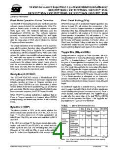
The Erase-Suspend operation temporarily suspends a
Sector- or Block-Erase operation thus allowing data to be
read from any memory location, or program data into any
sector/block that is not suspended for an Erase operation.
The operation is executed by issuing a one-byte command
sequence with Erase-Suspend command (B0H). The
device automatically enters read mode within 20 µs after
the Erase-Suspend command had been issued. Valid data
can be read from any sector or block that is not suspended
from an Erase operation. Reading at address location
within erase-suspended sectors/blocks will output DQ2 tog-
gling and DQ6 at “1”. While in Erase-Suspend mode, a
Word-/Byte-Program operation is allowed except for the
sector or block selected for Erase-Suspend. To resume
Sector-Erase or Block-Erase operation which has been
suspended, the system must issue an Erase-Resume
command. The operation is executed by issuing a one-byte
command sequence with Erase Resume command (30H)
at any address in the one-byte sequence.
See Figures 9 and 10 for WE# and BEF# controlled Pro-
gram operation timing diagrams and Figure 22 for flow-
charts. During the Program operation, the only valid reads
are Data# Polling and Toggle Bit. During the internal Pro-
gram operation, the host is free to perform additional tasks.
Any commands issued during an internal Program opera-
tion are ignored.
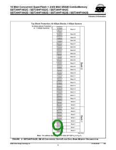
Flash Sector- (Block-) Erase Operation
These devices offer both Sector-Erase and Block-Erase
operations. These operations allow the system to erase the
devices on a sector-by-sector (or block-by-block) basis.
The sector architecture is based on a uniform sector size of
2 KWord. The Block-Erase mode is based on a uniform
block size of 32 KWord. The Sector-Erase operation is initi-
ated by executing a six-byte command sequence with a
Sector-Erase command (30H) and sector address (SA) in
the last bus cycle. The Block-Erase operation is initiated by
executing a six-byte command sequence with Block-Erase
command (50H) and block address (BA) in the last bus
cycle. The sector or block address is latched on the falling
edge of the sixth WE# pulse, while the command (30H or
50H) is latched on the rising edge of the sixth WE# pulse.
The internal Erase operation begins after the sixth WE#
pulse. Any commands issued during the Block- or Sector-
Erase operation are ignored except Erase-Suspend and
Erase-Resume. See Figures 14 and 15 for timing wave-
forms.
©2004 Silicon Storage Technology, Inc.
S71256-00-000
3/04
3

 SST [ SILICON STORAGE TECHNOLOGY, INC ]