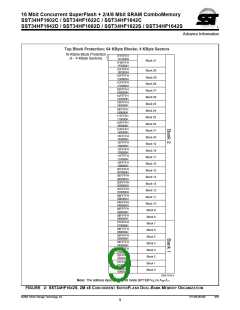
16 Mbit Concurrent SuperFlash + 2/4/8 Mbit SRAM ComboMemory
SST34HF1602C / SST34HF1622C / SST34HF1642C
SST34HF1642D / SST34HF1682D / SST34HF1622S / SST34HF1642S
Advance Information
Flash Write Operation Status Detection
Flash Data# Polling (DQ7)
The SST34HF16x2C/D/S provide one hardware and two
software means to detect the completion of a Write (Pro-
gram or Erase) cycle, in order to optimize the system
Write cycle time. The hardware detection uses the
Ready/Busy# (RY/BY#) pin. The software detection
includes two status bits: Data# Polling (DQ7) and Toggle
Bit (DQ6). The End-of-Write detection mode is enabled
after the rising edge of WE#, which initiates the internal
Program or Erase operation.
When the devices are in an internal Program operation, any
attempt to read DQ7 will produce the complement of the
true data. Once the Program operation is completed, DQ7
will produce true data. During internal Erase operation, any
attempt to read DQ7 will produce a ‘0’. Once the internal
Erase operation is completed, DQ7 will produce a ‘1’. The
Data# Polling is valid after the rising edge of fourth WE# (or
BEF#) pulse for Program operation. For Sector-, Block-, or
Chip-Erase, the Data# Polling is valid after the rising edge
of sixth WE# (or BEF#) pulse. See Figure 11 for Data# Poll-
ing (DQ7) timing diagram and Figure 23 for a flowchart.
The actual completion of the nonvolatile write is asynchro-
nous with the system; therefore, either a Ready/Busy# (RY/
BY#), Data# Polling (DQ7) or Toggle Bit (DQ6) read may be
simultaneous with the completion of the Write cycle. If this
occurs, the system may possibly get an erroneous result,
i.e., valid data may appear to conflict with either DQ7 or
DQ6. In order to prevent spurious rejection, if an erroneous
result occurs, the software routine should include a loop to
read the accessed location an additional two (2) times. If
both reads are valid, then the device has completed the
Write cycle, otherwise the rejection is valid.
Toggle Bits (DQ6 and DQ2)
During the internal Program or Erase operation, any con-
secutive attempts to read DQ6 will produce alternating “1”s
and “0”s, i.e., toggling between 1 and 0. When the internal
Program or Erase operation is completed, the DQ6 bit will
stop toggling. The device is then ready for the next opera-
tion. The toggle bit is valid after the rising edge of the fourth
WE# (or BEF#) pulse for Program operations. For Sector-,
Block-, or Chip-Erase, the toggle bit (DQ6) is valid after the
rising edge of sixth WE# (or BEF#) pulse. DQ6 will be set to
“1” if a Read operation is attempted on an Erase-sus-
pended Sector/Block. If Program operation is initiated in a
sector/block not selected in Erase-Suspend mode, DQ6 will
toggle.
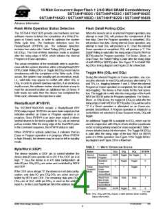
Ready/Busy# (RY/BY#)
The SST34HF16x2C/D/S include a Ready/Busy# (RY/
BY#) output signal. RY/BY# is an open drain output pin that
indicates whether an Erase or Program operation is in
progress. Since RY/BY# is an open drain output, it allows
several devices to be tied in parallel to VDD via an external
pull-up resistor. After the rising edge of the final WE# pulse
in the command sequence, the RY/BY# status is valid.
An additional Toggle Bit is available on DQ2, which can be
used in conjunction with DQ6 to check whether a particular
sector is being actively erased or erase-suspended. Table 1
shows detailed status bit information. The Toggle Bit (DQ2)
is valid after the rising edge of the last WE# (or BEF#)
pulse of a Write operation. See Figure 12 for Toggle Bit tim-
ing diagram and Figure 23 for a flowchart.
When RY/BY# is actively pulled low, it indicates that an
Erase or Program operation is in progress. When RY/BY#
is high (Ready), the devices may be read or left in standby
mode.
TABLE 1: WRITE OPERATION STATUS
Byte/Word (CIOF)
Status
DQ7
DQ6
DQ2
RY/BY#
The device includes a CIOF pin to control whether the
device data I/O pins operate x8 or x16. If the CIOF pin is at
logic “1” (VIH) the device is in x16 data configuration: all
data I/0 pins DQ0-DQ15 are active and controlled by BEF#
and OE#.
Normal
Operation Program
Standard
DQ7# Toggle No Toggle
0
Standard
Erase
0
1
Toggle
1
Toggle
Toggle
0
1
Erase-
Suspend Erase
Mode Suspended
Read From
If the CIOF pin is at logic “0”, the device is in x8 data config-
uration: only data I/O pins DQ0-DQ7 are active and con-
trolled by BEF# and OE#. The remaining data pins DQ8-
DQ14 are at Hi-Z, while pin DQ15 is used as the address
input A-1 for the Least Significant Bit of the address bus.
Sector/Block
Read From
Non-Erase
Suspended
Sector/Block
Data
Data
Data
N/A
1
Program
DQ7# Toggle
0
T1.0 1256
Note: DQ7, DQ6, and DQ2 require a valid address when reading
status information.
©2004 Silicon Storage Technology, Inc.
S71256-00-000
3/04
4

 SST [ SILICON STORAGE TECHNOLOGY, INC ]