16 Mbit Concurrent SuperFlash + 2/4/8 Mbit SRAM ComboMemory
SST34HF1602C / SST34HF1622C / SST34HF1642C
SST34HF1642D / SST34HF1682D / SST34HF1622S / SST34HF1642S
Advance Information
protect against inadvertent
SST34HF16x2C/D/S devices contain on-chip hardware
and software data protection schemes.
flash
write,
the
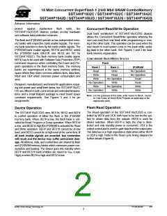
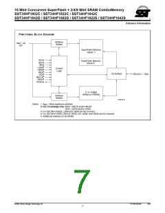
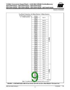
Concurrent Read/Write Operation
Dual bank architecture of SST34HF16x2C/D/S devices
allows the Concurrent Read/Write operation whereby the
user can read from one bank while programming or eras-
ing in the other bank. This operation can be used when the
user needs to read system code in one bank while updat-
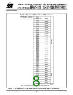
ing data in the other bank. See Figures 1 and 2 for dual-
bank memory organization.
The flash and (P)SRAM operate as two independent mem-
ory banks with respective bank enable signals. The mem-
ory bank selection is done by two bank enable signals. The
(P)SRAM bank enable signals, BES1# and BES2, select
the (P)SRAM bank (BES1# and BES2 are NC for
SST34HF1602C). The flash memory bank enable signal,
BEF#, has to be used with Software Data Protection (SDP)
command sequence when controlling the Erase and Pro-
gram operations in the flash memory bank. The memory
banks are superimposed in the same memory address
space where they share common address lines, data lines,
WE# and OE# which minimize power consumption and
area.
CONCURRENT READ/WRITE STATES
Flash
Bank 1
Read
Bank 2
Write
(P)SRAM
No Operation
No Operation
Read
Write
Read
Write
No Operation
Write
No Operation
Write
Read
Designed, manufactured, and tested for applications requir-
ing low power and small form factor, the SST34HF16x2C/
D/S are offered in both commercial and extended tempera-
tures and a small footprint package to meet board space
constraint requirements. See Figures 3 and 4 for pin
assignments.
No Operation
Write
Write
No Operation
Write
Note: For the purposes of this table, write means to Block-, Sector,
or Chip-Erase, or Word-/Byte-Program as applicable to the
appropriate bank.
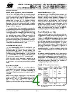
Flash Read Operation
Device Operation
The Read operation of the SST34HF16x2C/D/S is con-
trolled by BEF# and OE#, both have to be low for the sys-
tem to obtain data from the outputs. BEF# is used for
device selection. When BEF# is high, the chip is dese-
lected and only standby power is consumed. OE# is the
output control and is used to gate data from the output pins.
The data bus is in high impedance state when either BEF#
or OE# is high. Refer to the Read cycle timing diagram for
further details (Figure 8).
The SST34HF16x2C/D/S uses BES1#, BES2 and BEF#
to control operation of either the flash or the (P)SRAM
memory bank. When BEF# is low, the flash bank is acti-
vated for Read, Program or Erase operation. When BES1#
is low, and BES2 is high the (P)SRAM is activated for Read
and Write operation. BEF# and BES1# cannot be at low
level, and BES2 cannot be at high level at the same time. If
all bank enable signals are asserted, bus contention
will result and the device may suffer permanent dam-
age. All address, data, and control lines are shared by flash
and (P)SRAM memory banks which minimizes power con-
sumption and loading. The device goes into standby when
BEF# and BES1# bank enables are raised to VIHC (Logic
High) or when BEF# is high and BES2 is low.
©2004 Silicon Storage Technology, Inc.
S71256-00-000
3/04
2

 SST [ SILICON STORAGE TECHNOLOGY, INC ]