2 Mbit Page-Mode EEPROM
SST29EE020 / SST29LE020 / SST29VE020
Data Sheet
Product Identification
Product Identification Mode Exit
The product identification mode identifies the device as the
SST29EE/LE/VE020 and manufacturer as SST. This mode
is accessed via software. For details, see Table 4, Figure
11 for the software ID entry and read timing diagram, and
Figure 18 for the ID entry command sequence flowchart.
In order to return to the standard read mode, the Software
Product Identification mode must be exited. Exiting is
accomplished by issuing the Software ID Exit (reset) opera-
tion, which returns the device to the Read operation. The
Reset operation may also be used to reset the device to the
Read mode after an inadvertent transient condition that
apparently causes the device to behave abnormally, e.g.,
not read correctly. See Table 4 for software command
codes, Figure 12 for timing waveform, and Figure 18 for a
flowchart.
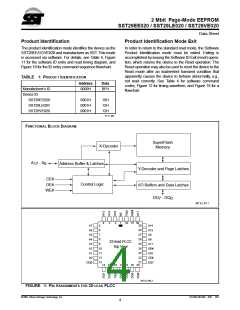
TABLE 1: PRODUCT IDENTIFICATION
Address
Data
Manufacturer’s ID
Device ID
0000H
BFH
SST29EE020
SST29LE020
SST29VE020
0001H
0001H
0001H
10H
12H
12H
T1.3 307
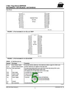
FUNCTIONAL BLOCK DIAGRAM
SuperFlash
Memory
X-Decoder
A
- A
0
17
Address Buffer & Latches
Control Logic
Y-Decoder and Page Latches
I/O Buffers and Data Latches
CE#
OE#
WE#
DQ - DQ
7
0
307 ILL B1.1
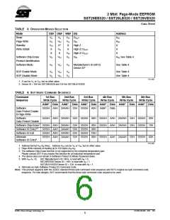
4
3
2
1
32 31 30
29
5
A7
A6
A14
A13
A8
6
28
27
26
25
24
23
22
21
7
A5
8
A4
A9
32-lead PLCC
Top View
9
A3
A11
10
11
12
13
A2
OE#
A10
CE#
DQ7
A1
A0
DQ0
14 15 16 17 18 19 20
307 ILL F02.3
FIGURE 1: PIN ASSIGNMENTS FOR 32-LEAD PLCC
©2001 Silicon Storage Technology, Inc.
S71062-06-000 6/01 307
4

 SST [ SILICON STORAGE TECHNOLOGY, INC ]