A d v a n c e I n f o r m a t i o n
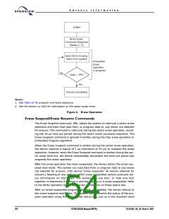
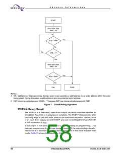
START
Read DQ7–DQ0
Addr = VA
Yes
DQ7 = Data?
No
No
DQ5 = 1?
Yes
Read DQ7–DQ0
Addr = VA
Yes
DQ7 = Data?
No
PASS
FAIL
Notes:
1. VA = Valid address for programming. During a sector erase operation, a valid address is any sector address within the sector
being erased. During chip erase, a valid address is any non-protected sector address.
2. DQ7 should be rechecked even if DQ5 = “1” because DQ7 may change simultaneously with DQ5.
Figure 7. Data# Polling Algorithm
RY/BY#: Ready/Busy#
The RY/BY# is a dedicated, open-drain output pin which indicates whether an
Embedded Algorithm is in progress or complete. The RY/BY# status is valid after
the rising edge of the final WE# pulse in the command sequence. Since RY/BY#
is an open-drain output, several RY/BY# pins can be tied together in parallel with
a pull-up resistor to VCC
.
If the output is low (Busy), the device is actively erasing or programming. (This
includes programming in the Erase Suspend mode.) If the output is high (Ready),
the device is in the read mode, the standby mode, or in the erase-suspend-read
mode. Table 23 shows the outputs for RY/BY#.
58
S71GL032A Based MCPs
S71GL032A_00_A0 March 31, 2005

 SPANSION [ SPANSION ]