P R E L I M I N A R Y
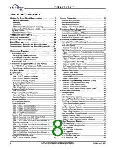
TABLE OF CONTENTS
Notice On Data Sheet Designations . . . . . . . . . . . 3
Advance Information .............................................................. 3
Preliminary ..........................................................................................................3
Combination .......................................................................................................3
Full Production (No Designation on Document) ...................................3
Simultaneous Read/Write Operation with Zero Latency ........................4
Page Mode Features .............................................................................................5
Standard Flash Memory Features .....................................................................5
TABLE OF CONTENTS . . . . . . . . . . . . . . . . . . . . .7
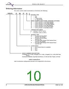
Ordering Information . . . . . . . . . . . . . . . . . . . . . . . 10
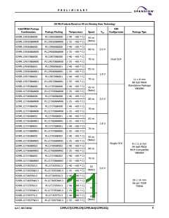
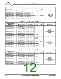
Product Selector Guide . . . . . . . . . . . . . . . . . . . . . 14
Block Diagram . . . . . . . . . . . . . . . . . . . . . . . . . . . 14
Sector Protection . . . . . . . . . . . . . . . . . . . . . . . . . 52
Persistent Sector Protection ........................................................................... 52
Password Sector Protection ........................................................................... 52
WP# Hardware Protection .............................................................................52
Selecting a Sector Protection Mode ............................................................. 52
Persistent Sector Protection . . . . . . . . . . . . . . . . 53
Persistent Protection Bit (PPB) ...................................................................... 53
Persistent Protection Bit Lock (PPB Lock) ................................................. 53
Dynamic Protection Bit (DYB) ....................................................................... 53
Persistent Sector Protection Mode Locking Bit ....................................... 55
Password Protection Mode . . . . . . . . . . . . . . . . . 55
Password and Password Mode Locking Bit ................................................ 55
64-bit Password ..................................................................................................56
Write Protect (WP#) .......................................................................................56
Persistent Protection Bit Lock ...................................................................56
High Voltage Sector Protection ..................................................................... 57
Figure 1. In-System Sector Protection/Sector Unprotection Algo-
rithms.............................................................................. 58
Temporary Sector Unprotect ........................................................................59
Figure 2. Temporary Sector Unprotect Operation ................... 59
SecSi™ (Secured Silicon) Sector Flash Memory Region ..........................59
Factory-Locked Area (64 words) ..............................................................59
Customer-Lockable Area (64 words) ......................................................60
SecSi Sector Protection Bits .......................................................................60
Figure 3. SecSi Sector Protect Verify.................................... 61
Hardware Data Protection ..............................................................................61
Low VCC Write Inhibit .................................................................................61
Write Pulse “Glitch” Protection ................................................................61
Logical Inhibit ....................................................................................................61
Power-Up Write Inhibit ................................................................................61
Simultaneous Read/Write Block Diagram . . . . . 15
Simultaneous Read/Write Block Diagram (PL129J)
. . . . . . . . . . . . . . . . . . . . . . . . . . . . . . . . . . . . . . . . . . 16
Connection Diagrams . . . . . . . . . . . . . . . . . . . . . . 17
80-Ball Fine-pitch BGA .......................................................................................17
Special Package Handling Instructions .......................................................17
64-Ball Fine-pitch BGA—MCP Compatible ................................................18
Special Package Handling Instructions ...................................................... 18
48-Ball Fine-pitch BGA ...................................................................................... 19
Connection Diagram (PL064J and PL032J) . . . . . .20
56-pin TSOP 20 x 14 mm Configuration (PL127J) ...................................... 21
Special Package Handling Instructions ...................................................... 21
Pin Description . . . . . . . . . . . . . . . . . . . . . . . . . . . .22
Logic Symbol . . . . . . . . . . . . . . . . . . . . . . . . . . . . 22
Device Bus Operations . . . . . . . . . . . . . . . . . . . . . .23
Table 1. PL127J Device Bus Operations ................................ 23
Table 2. PL129J Device Bus Operations ................................ 23
Requirements for Reading Array Data ........................................................ 24
Random Read (Non-Page Read) ............................................................... 24
Page Mode Read ............................................................................................. 24
Table 3. Page Select .......................................................... 24
Simultaneous Read/Write Operation ...........................................................25
Table 4. Bank Select .......................................................... 25
Writing Commands/Command Sequences .................................................25
Accelerated Program Operation .............................................................. 26
Autoselect Functions .................................................................................... 26
Automatic Sleep Mode ..................................................................................... 26
RESET#: Hardware Reset Pin .........................................................................27
Output Disable Mode ........................................................................................27
Table 5. PL127J Sector Architecture ..................................... 28
Table 6. PL064J Sector Architecture ..................................... 35
Table 7. PL032J Sector Architecture ..................................... 38
Table 8. S29PL129J Sector Architecture ............................... 40
Table 9. SecSiTM Sector Addresses ...................................... 46
Autoselect Mode ................................................................................................ 46
Table 10. Autoselect Codes (High Voltage Method) ................ 47
Table 11. Autoselect Codes for PL129J ................................. 47
Table 12. PL127J Boot Sector/Sector Block Addresses for
Common Flash Memory Interface (CFI) . . . . . . 62
Table 17. CFI Query Identification String .............................. 62
Table 18. System Interface String ........................................ 63
Table 19. Device Geometry Definition ................................... 63
Table 20. Primary Vendor-Specific Extended Query ................ 64
Command Definitions . . . . . . . . . . . . . . . . . . . . . .66
Reading Array Data ...........................................................................................66
Reset Command .................................................................................................66
Autoselect Command Sequence ....................................................................67
Enter SecSi™ Sector/Exit SecSi Sector Command Sequence ................67
Word Program Command Sequence ...........................................................67
Unlock Bypass Command Sequence ........................................................68
Figure 4. Program Operation............................................... 69
Chip Erase Command Sequence ...................................................................69
Sector Erase Command Sequence ................................................................70
Figure 5. Erase Operation................................................... 71
Erase Suspend/Erase Resume Commands ...................................................71
Command Definitions Tables ......................................................................... 73
Table 21. Memory Array Command Definitions ...................... 73
Table 22. Sector Protection Command Definitions .................. 75
Write Operation Status . . . . . . . . . . . . . . . . . . . . 76
DQ7: Data# Polling ............................................................................................76
Figure 6. Data# Polling Algorithm........................................ 77
DQ6: Toggle Bit I ...............................................................................................78
Figure 7. Toggle Bit Algorithm............................................. 79
DQ2: Toggle Bit II ..............................................................................................79
Reading Toggle Bits DQ6/DQ2 .....................................................................79
DQ5: Exceeded Timing Limits ........................................................................80
DQ3: Sector Erase Timer ................................................................................80
Protection/Unprotection ..................................................... 48
Table 13. PL129J Boot Sector/Sector Block Addresses for
Protection/Unprotection ..................................................... 49
Table 14. PL064J Boot Sector/Sector Block Addresses for
Protection/Unprotection ..................................................... 50
Table 15. PL032J Boot Sector/Sector Block Addresses for
Protection/Unprotection ..................................................... 51
Selecting a Sector Protection Mode ...............................................................51
Table 16. Sector Protection Schemes ................................... 52
6
S29PL127J/S29PL129J/S29PL064J/S29PL032J
31107A62 April 7, 2005

 SPANSION [ SPANSION ]