P R E L I M I N A R Y
General Description
The PL127J/PL129J/PL064J/PL032J is a 128/128/64/32 Mbit, 3.0 volt-only Page
Mode and Simultaneous Read/Write Flash memory device organized as 8/8/4/2
Mwords. The devices are offered in the following packages:
11mm x 8mm, 80-ball Fine-pitch BGA standalone (PL127J and PL129J)
8mm 11.6mm, 64-ball Fine-pitch BGA multi-chip compatible
x
(PL127J/PL129J)
8.15mm x 6.15mm, 48-ball Fine-pitch BGA standalone (PL064J/PL032J)
7mm x 9mm, 56-ball Fine-pitch BGA multi-chip compatible (PL064J and
PL032J)
20mm x 14mm, 56-pin TSOP (PL127J)
The word-wide data (x16) appears on DQ15-DQ0. This device can be pro-
grammed in-system or in standard EPROM programmers. A 12.0 V VPP is not
required for write or erase operations.
The device offers fast page access times of 20 to 30 ns, with corresponding ran-
dom access times of 55 to 70 ns, respectively, allowing high speed
microprocessors to operate without wait states. To eliminate bus contention the
device has separate chip enable (CE#), write enable (WE#) and output enable
(OE#) controls. Note: Device PL129J has 2 chip enable inputs (CE1#, CE2#).
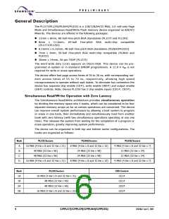
Simultaneous Read/Write Operation with Zero Latency
The Simultaneous Read/Write architecture provides simultaneous operation
by dividing the memory space into 4 banks, which can be considered to be four
separate memory arrays as far as certain operations are concerned. The device
can improve overall system performance by allowing a host system to program
or erase in one bank, then immediately and simultaneously read from another
bank with zero latency (with two simultaneous operations operating at any one
time). This releases the system from waiting for the completion of a program or
erase operation, greatly improving system performance.
The device can be organized in both top and bottom sector configurations. The
banks are organized as follows:
Bank
A
PL127J Sectors
PL064J Sectors
PL032J Sectors
16 Mbit (4 Kw x 8 and 32 Kw x 31)
48 Mbit (32 Kw x 96)
8 Mbit (4 Kw x 8 and 32 Kw x 15)
24 Mbit (32 Kw x 48)
4 Mbit (4 Kw x 8 and 32 Kw x 7)
12 Mbit (32 Kw x 24)
B
C
48 Mbit (32 Kw x 96)
24 Mbit (32 Kw x 48)
12 Mbit (32 Kw x 24)
D
16 Mbit (4 Kw x 8 and 32 Kw x 31)
8 Mbit (4 Kw x 8 and 32 Kw x 15)
4 Mbit (4 Kw x 8 and 32 Kw x 7)
Bank
1A
PL129J Sectors
CE# Control
CE1#
16 Mbit (4 Kw x 8 and 32 Kw x 31)
1B
48 Mbit (32 Kw x 96)
48 Mbit (32 Kw x 96)
CE1#
2A
CE2#
2B
16 Mbit (4 Kw x 8 and 32 Kw x 31)
CE2#
4
S29PL127J/S29PL129J/S29PL064J/S29PL032J
31107A62 April 7, 2005

 SPANSION [ SPANSION ]