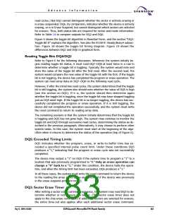
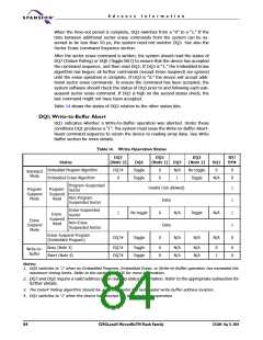
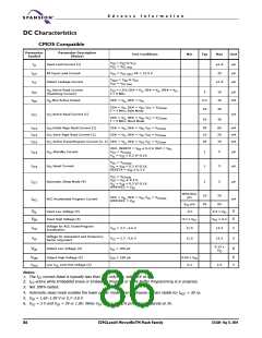
A d v a n c e I n f o r m a t i o n
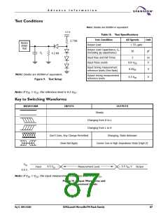
Test Conditions
Note: Diodes are IN3064 or equivalent
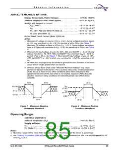
3.3 V
Table 15. Test Specifications
Test Condition
All Speeds
1 TTL gate
Unit
2.7 kΩ
Device
Under
Test
Output Load
Output Load Capacitance, CL
(including jig capacitance)
30
pF
C
L
6.2 kΩ
Input Rise and Fall Times
Input Pulse Levels
5
ns
V
0.0–VIO
Input timing measurement
reference levels (See Note)
0.5VIO
V
V
Note: Diodes are IN3064 or equivalent.
Output timing measurement
reference levels
0.5 VIO
Figure 9. Test Setup
Note: If VIO < VCC, the reference level is 0.5 VIO
.
Key to Switching Waveforms
WAVEFORM
INPUTS
OUTPUTS
Steady
Changing from H to L
Changing from L to H
Don’t Care, Any Change Permitted
Does Not Apply
Changing, State Unknown
Center Line is High Impedance State (High Z)
VIO
0.5 VIO
0.5 VIO V
Input
Measurement Level
Output
0.0 V
Note: If VIO < VCC, the input measurement reference level is 0.5 VIO
.
Figure 10. Input Waveforms and
Measurement Levels
May 13, 2004 27631A4
S29GLxxxN MirrorBitTM Flash Family
87

 SPANSION [ SPANSION ]