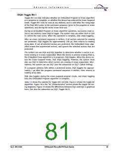
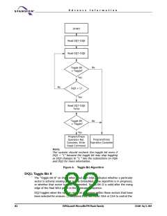
A d v a n c e I n f o r m a t i o n
ABSOLUTE MAXIMUM RATINGS
Storage Temperature, Plastic Packages. . . . . . . . . . . . . . . . –65°C to +150°C
Ambient Temperature with Power Applied . . . . . . . . . . . . . . –65°C to +125°C
Voltage with Respect to Ground:
VCC (Note 1). . . . . . . . . . . . . . . . . . . . . . . . . . . . . . .–0.5 V to +4.0 V
VIO . . . . . . . . . . . . . . . . . . . . . . . . . . . . . . . . . . . . .–0.5 V to +4.0 V
A9, OE#, ACC and RESET# (Note 2) . . . . . . . . . . . . .–0.5 V to +12.5 V
All other pins (Note 1). . . . . . . . . . . . . . . . . . . . . . .–0.5 V to +12.5 V
Output Short Circuit Current (Note 3)200 mA
Notes:
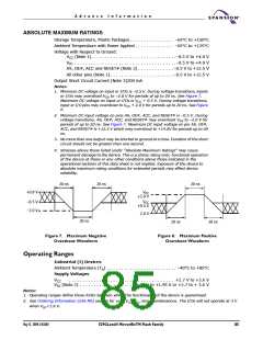
1. Minimum DC voltage on input or I/Os is –0.5 V. During voltage transitions, inputs
or I/Os may overshoot V to –2.0 V for periods of up to 20 ns. See Figure 7.
SS
Maximum DC voltage on input or I/Os is V + 0.5 V. During voltage transitions,
CC
input or I/O pins may overshoot to V + 2.0 V for periods up to 20 ns. See Figure
CC
8.
2. Minimum DC input voltage on pins A9, OE#, ACC, and RESET# is –0.5 V. During
voltage transitions, A9, OE#, ACC, and RESET# may overshoot V to –2.0 V for
SS
periods of up to 20 ns. See Figure 7. Maximum DC input voltage on pin A9, OE#,
ACC, and RESET# is +12.5 V which may overshoot to +14.0V for periods up to 20
ns.
3. No more than one output may be shorted to ground at a time. Duration of the short
circuit should not be greater than one second.
4. Stresses above those listed under “Absolute Maximum Ratings” may cause
permanent damage to the device. This is a stress rating only; functional operation
of the device at these or any other conditions above those indicated in the
operational sections of this data sheet is not implied. Exposure of the device to
absolute maximum rating conditions for extended periods may affect device
reliability.
20 ns
20 ns
20 ns
VCC
+2.0 V
+0.8 V
VCC
–0.5 V
–2.0 V
+0.5 V
2.0 V
20 ns
20 ns
20 ns
Figure 7. Maximum Negative
Overshoot Waveform
Figure 8. Maximum Positive
Overshoot Waveform
Operating Ranges
Industrial (I) Devices
Ambient Temperature (TA) . . . . . . . . . . . . . . . . . . . . . . . . . –40°C to +85°C
Supply Voltages
VCC
. . . . . . . . . . . . . . . . . . . . . . . . . . . . . . . . . . . . . . +2.7 V to +3.6 V
VIO (Note 2) . . . . . . . . . . . . . . . . . . . +1.65 V to +1.95 V or +2.7 to + 3.6 V
Notes:
1. Operating ranges define those limits between which the functionality of the device is guaranteed.
2. See Ordering Information (256 Mb) section for valid V /V range combinations. The I/Os will not operate at 3 V
CC IO
when V =1.8 V.
IO
May 13, 2004 27631A4
S29GLxxxN MirrorBitTM Flash Family
85

 SPANSION [ SPANSION ]