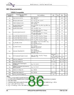
A d v a n c e I n f o r m a t i o n
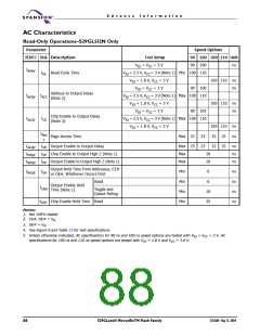
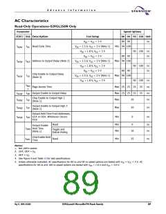
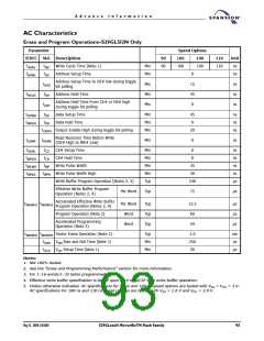
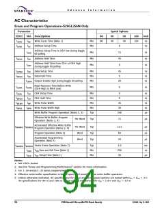
AC Characteristics
Read-Only Operations–S29GL128N Only
Parameter
Speed Options
JEDEC Std. Description
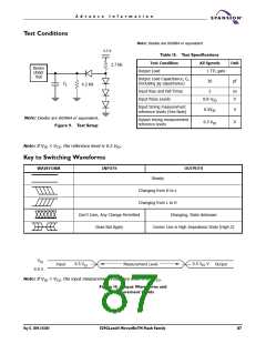
Test Setup
VIO = VCC = 3 V
80 90 90 100 Unit
80
90
ns
tAVAV
tAVQV
tELQV
tRC Read Cycle Time
VIO = 2.5 V, VCC = 3 V (Note 1) Min
VIO = 1.8 V, VCC = 3 V
90 100
90 100
90 100
90 100
ns
ns
VIO = VCC = 3 V
80
90
tACC Address to Output Delay (Note 2)
tCE Chip Enable to Output Delay (Note 3)
VIO = 2.5 V, VCC = 3 V (Note 1) Max 90 100
VIO = 1.8 V, VCC = 3 V
ns
ns
VIO = VCC = 3 V
80
90
VIO = 2.5 V, VCC = 3 V (Note 1) Max 90 100
VIO = 1.8 V, VCC = 3 V
ns
ns
tPAC
Page Access Time
Max 25
25 35 35
C
tGLQV
tEHQZ
tGHQZ
tOE Output Enable to Output Delay
Max 25
Max
25 35 35
ns
ns
ns
tDF Chip Enable to Output High Z (Note 1)
tDF Output Enable to Output High Z (Note 1)
20
20
Max
Output Hold Time From Addresses, CE#
or OE#, Whichever Occurs First
tAXQX
tOH
Min
Min
Min
0
0
ns
ns
ns
Read
Output Enable Hold
tOEH
Toggle and
Data# Polling
Time (Note 1)
10
Chip Enable Hold
Time
tCEH
Read
Min
35
ns
Notes:
1. Not 100% tested.
2. CE#, OE# = VIL
3. OE# = VIL
4. See Figure 9 and Table 15 for test specifications.
5. Unless otherwise indicated, AC specifications for 80 ns and 90 ns speed options are tested with VIO = VCC = 3 V. AC
specifications for 90 ns and 100 ns speed options are tested with VIO = 1.8 V and VCC = 3.0 V.
90
S29GLxxxN MirrorBitTM Flash Family
27631A4 May 13, 2004

 SPANSION [ SPANSION ]