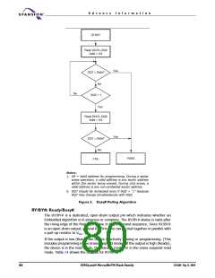
A d v a n c e I n f o r m a t i o n
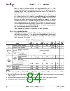
When the time-out period is complete, DQ3 switches from a “0” to a “1.” If the
time between additional sector erase commands from the system can be as-
sumed to be less than 50 µs, the system need not monitor DQ3. See also the
Sector Erase Command Sequence section.
After the sector erase command is written, the system should read the status of
DQ7 (Data# Polling) or DQ6 (Toggle Bit I) to ensure that the device has accepted
the command sequence, and then read DQ3. If DQ3 is “1,” the Embedded Erase
algorithm has begun; all further commands (except Erase Suspend) are ignored
until the erase operation is complete. If DQ3 is “0,” the device will accept addi-
tional sector erase commands. To ensure the command has been accepted, the
system software should check the status of DQ3 prior to and following each sub-
sequent sector erase command. If DQ3 is high on the second status check, the
last command might not have been accepted.
Table 14 shows the status of DQ3 relative to the other status bits.
DQ1: Write-to-Buffer Abort
DQ1 indicates whether a Write-to-Buffer operation was aborted. Under these
conditions DQ1 produces a “1”. The system must issue the Write-to-Buffer-Abort-
Reset command sequence to return the device to reading array data. See Write
Buffer section for more details.
Table 14. Write Operation Status
DQ7
(Note 2)
DQ5
(Note 1) DQ3
DQ2
(Note 2)
RY/
BY#
Status
DQ6
DQ1
0
Embedded Program Algorithm
Embedded Erase Algorithm
Program-Suspended
DQ7#
0
Toggle
Toggle
0
0
N/A
1
No toggle
Toggle
0
0
Standard
Mode
N/A
Invalid (not allowed)
Data
1
1
1
1
0
Program
Suspend
Mode
Program-
Suspend
Read
Sector
Non-Program
Suspended Sector
Erase-Suspended
Sector
1
No toggle
Toggle
0
N/A
Toggle
N/A
N/A
N/A
Erase-
Suspend
Read
Erase
Suspend
Mode
Non-Erase
Suspended Sector
Data
Erase-Suspend-Program
(Embedded Program)
DQ7#
0
N/A
Busy (Note 3)
Abort (Note 4)
DQ7#
DQ7#
Toggle
Toggle
0
0
N/A
N/A
N/A
N/A
0
1
0
0
Write-to-
Buffer
Notes:
1. DQ5 switches to ‘1’ when an Embedded Program, Embedded Erase, or Write-to-Buffer operation has exceeded the
maximum timing limits. Refer to the section on DQ5 for more information.
2. DQ7 and DQ2 require a valid address when reading status information. Refer to the appropriate subsection for
further details.
3. The Data# Polling algorithm should be used to monitor the last loaded write-buffer address location.
4. DQ1 switches to ‘1’ when the device has aborted the write-to-buffer operation
84
S29GLxxxN MirrorBitTM Flash Family
27631A4 May 13, 2004

 SPANSION [ SPANSION ]