A d v a n c e I n f o r m a t i o n
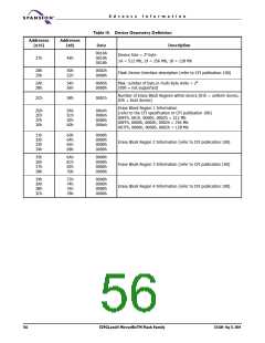
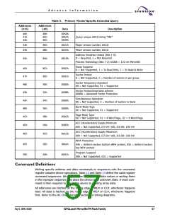
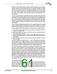
Table 11. Primary Vendor-Specific Extended Query
Addresses
(x16)
Addresses
(x8)
Data
Description
40h
41h
42h
80h
82h
84h
0050h
0052h
0049h
Query-unique ASCII string “PRI”
43h
44h
86h
88h
0031h
0033h
Major version number, ASCII
Minor version number, ASCII
Address Sensitive Unlock (Bits 1-0)
0 = Required, 1 = Not Required
45h
8Ah
0010h
Process Technology (Bits 7-2) 0100b = 110 nm MirrorBit
Erase Suspend
46h
47h
48h
49h
4Ah
4Bh
4Ch
8Ch
8Eh
90h
92h
94h
96h
98h
0002h
0001h
0000h
0008h
0000h
0000h
0002h
0 = Not Supported, 1 = To Read Only, 2 = To Read & Write
Sector Protect
0 = Not Supported, X = Number of sectors in per group
Sector Temporary Unprotect
00 = Not Supported, 01 = Supported
Sector Protect/Unprotect scheme
0008h = Advanced Sector Protection
Simultaneous Operation
00 = Not Supported, X = Number of Sectors in Bank
Burst Mode Type
00 = Not Supported, 01 = Supported
Page Mode Type
00 = Not Supported, 01 = 4 Word Page, 02 = 8 Word Page
ACC (Acceleration) Supply Minimum
4Dh
4Eh
9Ah
9Ch
00B5h
00C5h
00h = Not Supported, D7-D4: Volt, D3-D0: 100 mV
ACC (Acceleration) Supply Maximum
00h = Not Supported, D7-D4: Volt, D3-D0: 100 mV
WP# Protection
4Fh
50h
9Eh
A0h
00xxh
0001h
04h = Uniform sectors bottom WP# protect, 05h = Uniform sectors
top WP# protect
Program Suspend
00h = Not Supported, 01h = Supported
Command Definitions
Writing specific address and data commands or sequences into the command
register initiates device operations. Table 12 and Table 13 define the valid register
command sequences. Writing incorrect address and data values or writing them
in the improper sequence may place the device in an unknown state. A reset com-
mand is then required to return the device to reading array data.
All addresses are latched on the falling edge of WE# or CE#, whichever happens
later. All data is latched on the rising edge of WE# or CE#, whichever happens
first. Refer to the AC Characteristics section for timing diagrams.
May 13, 2004 27631A4
S29GLxxxN MirrorBitTM Flash Family
57

 SPANSION [ SPANSION ]