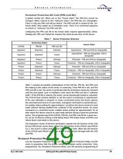
A d v a n c e I n f o r m a t i o n
Write Protect (WP#)
The Write Protect function provides a hardware method of protecting the first or
last sector group without using VID. Write Protect is one of two functions provided
by the WP#/ACC input.
If the system asserts VIL on the WP#/ACC pin, the device disables program and
erase functions in the first or last sector group independently of whether those
sector groups were protected or unprotected using the method described in“Ad-
vanced Sector Protection” section on page 46. Note that if WP#/ACC is at VIL
when the device is in the standby mode, the maximum input load current is in-
creased. See the table in “DC Characteristics” section on page 86.
If the system asserts VIH on the WP#/ACC pin, the device reverts to
whether the first or last sector was previously set to be protected or un-
protected using the method described in “Sector Group Protection and
Unprotection”. Note that WP# has an internal pullup; when uncon-
nected, WP# is at VIH
.
Hardware Data Protection
The command sequence requirement of unlock cycles for programming or erasing
provides data protection against inadvertent writes (refer to Tables 16 and 17 for
command definitions). In addition, the following hardware data protection mea-
sures prevent accidental erasure or programming, which might otherwise be
caused by spurious system level signals during VCC power-up and power-down
transitions, or from system noise.
Low V
Write Inhibit
CC
When VCC is less than VLKO, the device does not accept any write cycles. This pro-
tects data during VCC power-up and power-down. The command register and all
internal program/erase circuits are disabled, and the device resets to the read
mode. Subsequent writes are ignored until VCC is greater than VLKO. The system
must provide the proper signals to the control pins to prevent unintentional writes
when VCC is greater than VLKO
.
Write Pulse “Glitch” Protection
Noise pulses of less than 5 ns (typical) on OE#, CE# or WE# do not initiate a write
cycle.
Logical Inhibit
Write cycles are inhibited by holding any one of OE# = VIL, CE# = VIH or WE# =
VIH. To initiate a write cycle, CE# and WE# must be a logical zero while OE# is a
logical one.
Power-Up Write Inhibit
If WE# = CE# = VIL and OE# = VIH during power up, the device does not accept
commands on the rising edge of WE#. The internal state machine is automatically
reset to the read mode on power-up.
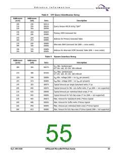
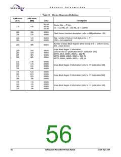
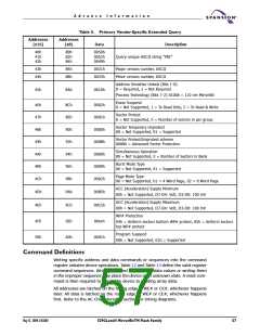
Common Flash Memory Interface (CFI)
The Common Flash Interface (CFI) specification outlines device and host system
software interrogation handshake, which allows specific vendor-specified soft-
ware algorithms to be used for entire families of devices. Software support can
May 13, 2004 27631A4
S29GLxxxN MirrorBitTM Flash Family
53

 SPANSION [ SPANSION ]