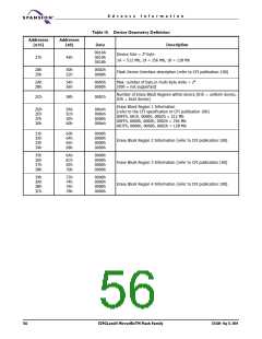
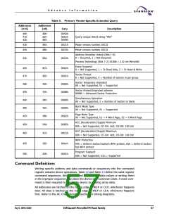
A d v a n c e I n f o r m a t i o n
compatibility with existing Flash driver software and for occassional writng of in-
dividual words. Use of Write Buffer Programming is strongly recommended for
general programming use when more than a few words are to be programmed.
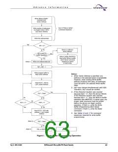
The effective word programming time using Write Buffer Programming is much
shorter than the single word programming time. Any word cannot be pro-
grammed from “0” back to a “1.” Attempting to do so may cause the device
to set DQ5 = 1, or cause the DQ7 and DQ6 status bits to indicate the operation
was successful. However, a succeeding read will show that the data is still “0.”
Only erase operations can convert a “0” to a “1.”
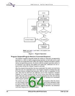
Unlock Bypass Command Sequence
The unlock bypass feature allows the system to program words to the device
faster than using the standard program command sequence. The unlock bypass
command sequence is initiated by first writing two unlock cycles. This is followed
by a third write cycle containing the unlock bypass command, 20h. The device
then enters the unlock bypass mode. A two-cycle unlock bypass program com-
mand sequence is all that is required to program in this mode. The first cycle in
this sequence contains the unlock bypass program command, A0h; the second
cycle contains the program address and data. Additional data is programmed in
the same manner. This mode dispenses with the initial two unlock cycles required
in the standard program command sequence, resulting in faster total program-
ming time. Table 12 and Table 13 show the requirements for the command
sequence.
During the unlock bypass mode, only the Unlock Bypass Program and Unlock By-
pass Reset commands are valid. To exit the unlock bypass mode, the system
must issue the two-cycle unlock bypass reset command sequence. (See Table 12
and Table 13).
Write Buffer Programming
Write Buffer Programming allows the system write to a maximum of 16 words/32
bytes in one programming operation. This results in faster effective programming
time than the standard programming algorithms. The Write Buffer Programming
command sequence is initiated by first writing two unlock cycles. This is followed
by a third write cycle containing the Write Buffer Load command written at the
Sector Address in which programming will occur. The fourth cycle writes the sec-
tor address and the number of word locations, minus one, to be programmed. For
example, if the system will program 6 unique address locations, then 05h should
be written to the device. This tells the device how many write buffer addresses
will be loaded with data and therefore when to expect the Program Buffer to Flash
command. The number of locations to program cannot exceed the size of the
write buffer or the operation will abort.
The fifth cycle writes the first address location and data to be programmed. The
write-buffer-page is selected by address bits AMAX–A4. All subsequent address/
data pairs must fall within the selected-write-buffer-page. The system then
writes the remaining address/data pairs into the write buffer. Write buffer loca-
tions may be loaded in any order.
The write-buffer-page address must be the same for all address/data pairs loaded
into the write buffer. (This means Write Buffer Programming cannot be performed
across multiple write-buffer pages. This also means that Write Buffer Program-
ming cannot be performed across multiple sectors. If the system attempts to load
programming data outside of the selected write-buffer page, the operation will
abort.)
60
S29GLxxxN MirrorBitTM Flash Family
27631A4 May 13, 2004

 SPANSION [ SPANSION ]