A d v a n c e I n f o r m a t i o n
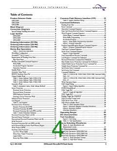
Table of Contents
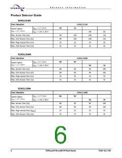
Product Selector Guide . . . . . . . . . . . . . . . . . . . . . .6
S29GL512N ..............................................................................................................6
S29GL256N .............................................................................................................6
S29GL128N ..............................................................................................................6
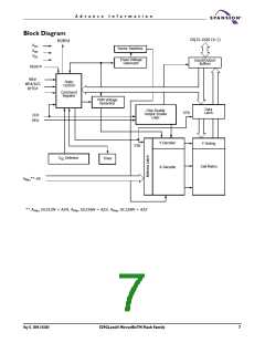
Block Diagram . . . . . . . . . . . . . . . . . . . . . . . . . . . . 7
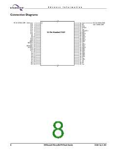
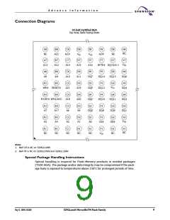
Connection Diagrams . . . . . . . . . . . . . . . . . . . . . . .8
Special Package Handling Instructions ............................................................9
Logic Symbol . . . . . . . . . . . . . . . . . . . . . . . . . . . . . . 11
S29GL512N ......................................................................................................... 11
S29GL256N ........................................................................................................ 11
S29GL128N ........................................................................................................ 11
Ordering Information (512 Mb) . . . . . . . . . . . . . . . 12
Ordering Information (256 Mb) . . . . . . . . . . . . . . . 13
Ordering Information (128 Mb) . . . . . . . . . . . . . . . 14
Device Bus Operations . . . . . . . . . . . . . . . . . . . . . . 15
Table 1. Device Bus Operations ........................................... 15
Word/Byte Configuration .................................................................................15
VersatileIOTM (VIO) Control ..............................................................................15
Requirements for Reading Array Data ......................................................... 16
Page Mode Read .............................................................................................. 16
Writing Commands/Command Sequences ................................................. 16
Write Buffer ......................................................................................................17
Accelerated Program Operation ................................................................17
Autoselect Functions ......................................................................................17
Standby Mode ........................................................................................................17
Automatic Sleep Mode .......................................................................................17
RESET#: Hardware Reset Pin ......................................................................... 18
Common Flash Memory Interface (CFI) . . . . . . . 53
Table 9. System Interface String.......................................... 55
Command Definitions . . . . . . . . . . . . . . . . . . . . . . 57
Reading Array Data ...........................................................................................58
Reset Command .................................................................................................58
Autoselect Command Sequence ...................................................................58
Enter SecSi Sector/Exit SecSi Sector Command Sequence ................... 59
Word Program Command Sequence .......................................................... 59
Unlock Bypass Command Sequence ........................................................60
Write Buffer Programming .........................................................................60
Accelerated Program .....................................................................................61
Figure 1. Write Buffer Programming Operation....................... 63
Figure 2. Program Operation ............................................... 64
Program Suspend/Program Resume Command Sequence ....................64
Figure 3. Program Suspend/Program Resume........................ 65
Chip Erase Command Sequence ................................................................... 65
Sector Erase Command Sequence ................................................................66
Figure 4. Erase Operation ................................................... 67
Erase Suspend/Erase Resume Commands .................................................. 67
Lock Register Command Set Definitions ....................................................68
Password Protection Command Set Definitions ......................................68
Non-Volatile Sector Protection Command Set Definitions ..................70
Global Volatile Sector Protection Freeze Command Set ......................70
Volatile Sector Protection Command Set ................................................... 71
SecSi Sector Entry Command .......................................................................... 71
SecSi Sector Exit Command ........................................................................... 72
Command Definitions ........................................................................................73
Table 12. S29GL512N, S29GL256N, S29GL128N Command Defini-
tions, x16 .........................................................................73
Table 13. S29GL512N, S29GL256N, S29GL128N Command Defini-
tions, x8 ...........................................................................76
Write Operation Status ...................................................................................78
DQ7: Data# Polling ...........................................................................................78
Figure 5. Data# Polling Algorithm ........................................ 80
RY/BY#: Ready/Busy# .......................................................................................80
DQ6: Toggle Bit I ................................................................................................81
Figure 6. Toggle Bit Algorithm ............................................. 82
DQ2: Toggle Bit II ..............................................................................................82
Reading Toggle Bits DQ6/DQ2 .....................................................................83
DQ5: Exceeded Timing Limits ........................................................................83
DQ3: Sector Erase Timer ................................................................................83
DQ1: Write-to-Buffer Abort ...........................................................................84
Table 14. Write Operation Status .........................................84
Figure 7. Maximum Negative Overshoot Waveform................. 85
Figure 8. Maximum Positive
Overshoot Waveform.......................................................... 85
Operating Ranges . . . . . . . . . . . . . . . . . . . . . . . . . 85
DC Characteristics . . . . . . . . . . . . . . . . . . . . . . . . 86
Test Conditions . . . . . . . . . . . . . . . . . . . . . . . . . . . 87
Figure 9. Test Setup........................................................... 87
Table 15. Test Specifications ...............................................87
Key to Switching Waveforms . . . . . . . . . . . . . . . . 87
Figure 10. Input Waveforms and
Output Disable Mode ........................................................................................ 18
Table 2. Sector Address Table–S29GL512N ........................... 18
Table 3. Sector Address Table–S29GL256N ........................... 33
Table 4. Sector Address Table–S29GL128N ........................... 40
Autoselect Mode ................................................................................................ 44
Table 5. Autoselect Codes, (High Voltage Method) ................ 45
Sector Protection ................................................................................................45
Persistent Sector Protection .......................................................................45
Password Sector Protection ........................................................................45
WP# Hardware Protection .........................................................................45
Selecting a Sector Protection Mode .........................................................45
Advanced Sector Protection .......................................................................... 46
Lock Register ....................................................................................................... 46
Table 6. Lock Register ........................................................ 47
Persistent Sector Protection ...........................................................................47
Dynamic Protection Bit (DYB) ...................................................................47
Persistent Protection Bit (PPB) .................................................................48
Persistent Protection Bit Lock (PPB Lock Bit) ..................................... 49
Table 7. Sector Protection Schemes ..................................... 49
Persistent Protection Mode Lock Bit .......................................................... 49
Password Sector Protection ........................................................................... 50
Password and Password Protection Mode Lock Bit ............................... 50
64-bit Password ....................................................................................................51
Persistent Protection Bit Lock (PPB Lock Bit) ............................................51
SecSi (Secured Silicon) Sector Flash Memory Region ...............................51
Write Protect (WP#) ........................................................................................53
Hardware Data Protection ..............................................................................53
Low VCC Write Inhibit ................................................................................53
Write Pulse “Glitch” Protection ................................................................53
Logical Inhibit ...................................................................................................53
Power-Up Write Inhibit ................................................................................53
Measurement Levels........................................................... 87
AC Characteristics . . . . . . . . . . . . . . . . . . . . . . . . 88
Read-Only Operations–S29GL512N Only ..................................................88
Read-Only Operations–S29GL256N Only .................................................89
Read-Only Operations–S29GL128N Only ..................................................90
Figure 11. Read Operation Timings....................................... 91
Figure 12. Page Read Timings.............................................. 91
May 13, 2004 27631A4
S29GLxxxN MirrorBitTM Flash Family
4

 SPANSION [ SPANSION ]