A d v a n c e I n f o r m a t i o n
General Description
The S29GL512/256/128N family of devices are 3.0V single power flash memory
manufactured using 110 nm MirrorBit technology. The S29GL512N is a 512 Mbit,
organized as 33,554,432 words or 67,108,864 bytes. The S29GL256N is a 256
Mbit, organized as 16,777,216 words or 33,554,432 bytes. The S29GL128N is a
128 Mbit, organized as 8,388,608 words or 16,777,216 bytes. The devices have
a 16-bit wide data bus that can also function as an 8-bit wide data bus by using
the BYTE# input. The device can be programmed either in the host system or in
standard EPROM programmers.
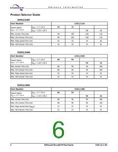
Access times as fast as 80 ns (S29GL128N, S29GL256N) or 90 ns (S29GL512N)
are available. Note that each access time has a specific operating voltage range
(VCC) and an I/O voltage range (VIO), as specified in the Product Selector Guide
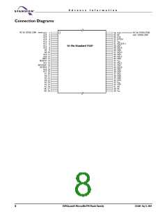
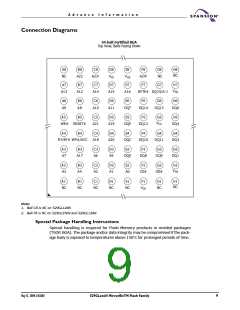
and the Ordering Information (512 Mb) sections. The devices are offered in a 56-
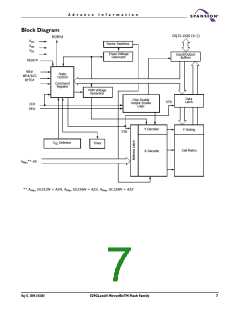
pin TSOP or 64-ball Fortified BGA package. Each device has separate chip enable
(CE#), write enable (WE#) and output enable (OE#) controls.
Each device requires only a single 3.0 volt power supply for both read and
write functions. In addition to a VCC input, a high-voltage accelerated program
(WP#/ACC) input provides shorter programming times through increased cur-
rent. This feature is intended to facilitate factory throughput during system
production, but may also be used in the field if desired.
The devices are entirely command set compatible with the JEDEC single-
power-supply Flash standard. Commands are written to the device using
standard microprocessor write timing. Write cycles also internally latch addresses
and data needed for the programming and erase operations.
The sector erase architecture allows memory sectors to be erased and repro-
grammed without affecting the data contents of other sectors. The device is fully
erased when shipped from the factory.
Device programming and erasure are initiated through command sequences.
Once a program or erase operation has begun, the host system need only poll the
DQ7 (Data# Polling) or DQ6 (toggle) status bits or monitor the Ready/Busy#
(RY/BY#) output to determine whether the operation is complete. To facilitate
programming, an Unlock Bypass mode reduces command sequence overhead
by requiring only two write cycles to program data instead of four.
The Enhanced VersatileI/O™ (VIO) control allows the host system to set the
voltage levels that the device generates and tolerates on all input levels (address,
chip control, and DQ input levels) to the same voltage level that is asserted on
the VIO pin. This allows the device to operate in a 1.8 V or 3 V system environ-
ment as required.
Hardware data protection measures include a low VCC detector that automat-
ically inhibits write operations during power transitions. Persistent Sector
Protection provides in-system, command-enabled protection of any combina-
tion of sectors using a single power supply at VCC. Password Sector Protection
prevents unauthorized write and erase operations in any combination of sectors
through a user-defined 64-bit password.
The Erase Suspend/Erase Resume feature allows the host system to pause an
erase operation in a given sector to read or program any other sector and then
complete the erase operation. The Program Suspend/Program Resume fea-
ture enables the host system to pause a program operation in a given sector to
read any other sector and then complete the program operation.
2
S29GLxxxN MirrorBitTM Flash Family
27631A4 May 13, 2004

 SPANSION [ SPANSION ]