A d v a n c e I n f o r m a t i o n
level that is asserted on VIO. See Ordering Information for VIO options on this
device.
For example, a VI/O of 1.65–3.6 volts allows for I/O at the 1.8 or 3 volt levels,
driving and receiving signals to and from other 1.8 or 3 V devices on the same
data bus.
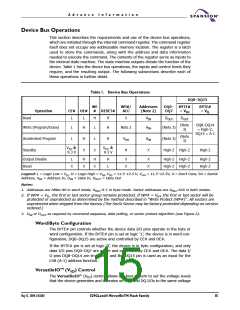
Requirements for Reading Array Data
To read array data from the outputs, the system must drive the CE# and OE#
pins to VIL. CE# is the power control and selects the device. OE# is the output
control and gates array data to the output pins. WE# should remain at VIH.
The internal state machine is set for reading array data upon device power-up,
or after a hardware reset. This ensures that no spurious alteration of the memory
content occurs during the power transition. No command is necessary in this
mode to obtain array data. Standard microprocessor read cycles that assert valid
addresses on the device address inputs produce valid data on the device data
outputs. The device remains enabled for read access until the command register
contents are altered.
See “Reading Array Data” for more information. Refer to the AC Read-Only Op-
erations table for timing specifications and to Figure 11 for the timing diagram.
Refer to the DC Characteristics table for the active current specification on read-
ing array data.
Page Mode Read
The device is capable of fast page mode read and is compatible with the page
mode Mask ROM read operation. This mode provides faster read access speed for
random locations within a page. The page size of the device is 8 words/16 bytes.
The appropriate page is selected by the higher address bits A(max)–A3. Address
bits A2–A0 in word mode (A2–A-1 in byte mode) determine the specific word
within a page. This is an asynchronous operation; the microprocessor supplies
the specific word location.
The random or initial page access is equal to tACC or tCE and subsequent page
read accesses (as long as the locations specified by the microprocessor falls
within that page) is equivalent to tPACC. When CE# is de-asserted and reasserted
for a subsequent access, the access time is tACC or tCE. Fast page mode accesses
are obtained by keeping the “read-page addresses” constant and changing the
“intra-read page” addresses.
Writing Commands/Command Sequences
To write a command or command sequence (which includes programming data
to the device and erasing sectors of memory), the system must drive WE# and
CE# to VIL, and OE# to VIH.
The device features an Unlock Bypass mode to facilitate faster programming.
Once the device enters the Unlock Bypass mode, only two write cycles are re-
quired to program a word or byte, instead of four. The “Word/Byte Program
Command Sequence” section has details on programming data to the device
using both standard and Unlock Bypass command sequences.
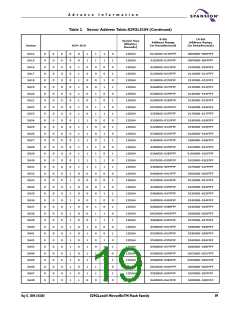
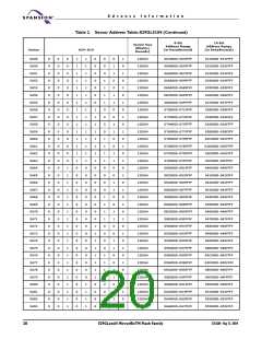
An erase operation can erase one sector, multiple sectors, or the entire device.
Table 2 indicates the address space that each sector occupies.
16
S29GLxxxN MirrorBitTM Flash Family
27631A4 May 13, 2004

 SPANSION [ SPANSION ]