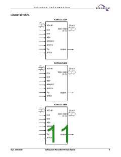
A d v a n c e I n f o r m a t i o n
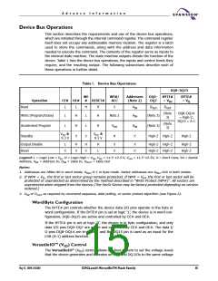
Device Bus Operations
This section describes the requirements and use of the device bus operations,
which are initiated through the internal command register. The command register
itself does not occupy any addressable memory location. The register is a latch
used to store the commands, along with the address and data information
needed to execute the command. The contents of the register serve as inputs to
the internal state machine. The state machine outputs dictate the function of the
device. Table 1 lists the device bus operations, the inputs and control levels they
require, and the resulting output. The following subsections describe each of
these operations in further detail.
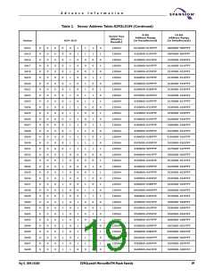
Table 1. Device Bus Operations
DQ8–DQ15
DQ0– BYTE# BYTE#
WE
#
WP#/
ACC
Addresses
(Note 2)
Operation
CE# OE#
RESET#
DQ7
= VIH
= VIL
Read
L
L
L
H
L
H
X
AIN
AIN
DOUT
DOUT
(Note
3)
DQ8–DQ14
= High-Z,
DQ15 = A-1
Write (Program/Erase)
Accelerated Program
Standby
H
H
H
Note 2
(Note 3)
(Note 3)
(Note
3)
L
H
X
L
VHH
H
AIN
X
VCC
0.3 V
±
VCC
0.3 V
±
X
High-Z High-Z
High-Z
Output Disable
Reset
L
H
X
H
X
H
L
X
X
X
X
High-Z High-Z
High-Z High-Z
High-Z
High-Z
X
Legend: L = Logic Low = V , H = Logic High = V , V = 11.5–12.5 V, V = 11.5–12.5V, X = Don’t Care, SA = Sector
IL
IH
ID
HH
Address, A = Address In, D = Data In, D = Data Out
IN
IN
OUT
Notes:
1. Addresses are AMax:A0 in word mode; A
:A-1 in byte mode. Sector addresses are A
:A16 in both modes.
Max
Max
2. If WP# = VIL, the first or last sector group remains protected. If WP# = VIH, the first or last sector will be
protected or unprotected as determined by the method described in “Write Protect (WP#)”. All sectors are
unprotected when shipped from the factory (The SecSi Sector may be factory protected depending on version
ordered.)
3. D or D
as required by command sequence, data polling, or sector protect algorithm (see Figure 2).
OUT
IN
Word/Byte Configuration
The BYTE# pin controls whether the device data I/O pins operate in the byte or
word configuration. If the BYTE# pin is set at logic ‘1’, the device is in word con-
figuration, DQ0–DQ15 are active and controlled by CE# and OE#.
If the BYTE# pin is set at logic ‘0’, the device is in byte configuration, and only
data I/O pins DQ0–DQ7 are active and controlled by CE# and OE#. The data I/
O pins DQ8–DQ14 are tri-stated, and the DQ15 pin is used as an input for the
LSB (A-1) address function.
VersatileIOTM (V ) Control
IO
The VersatileIOTM (VIO) control allows the host system to set the voltage levels
that the device generates and tolerates on CE# and DQ I/Os to the same voltage
May 13, 2004 27631A4
S29GLxxxN MirrorBitTM Flash Family
15

 SPANSION [ SPANSION ]