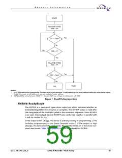
A d v a n c e I n f o r m a t i o n
In all these cases, the system must write the reset command to return the device
to the reading the array (or to erase-suspend-read if the device was previously
in the erase-suspend-program mode).
DQ3: Sector Erase Timer
After writing a sector erase command sequence, the system may read DQ3 to
determine whether or not erasure began. (The sector erase timer does not apply
to the chip erase command.) If additional sectors are selected for erasure, the
entire time-out also applies after each additional sector erase command. When
the time-out period is complete, DQ3 switches from a 0 to a 1. If the time be-
tween additional sector erase commands from the system can be assumed to be
less than 50 µs, the system need not monitor DQ3. See also the Sector Erase
Command Sequence section.
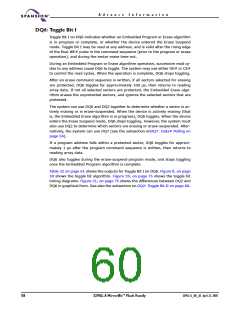
After the sector erase command is written, the system should read the status of
DQ7 (Data# Polling) or DQ6 (Toggle Bit I) to ensure that the device accepted the
command sequence, and then read DQ3. If DQ3 is 1, the Embedded Erase algo-
rithm has begun; all further commands (except Erase Suspend) are ignored until
the erase operation is complete. If DQ3 is 0, the device accepts additional sector
erase commands. To ensure the command is accepted, the system software
should check the status of DQ3 prior to and following each subsequent sector
erase command. If DQ3 is high on the second status check, the last command
might not have been accepted.
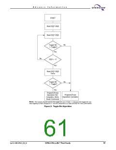
Table 32 on page 61 shows the status of DQ3 relative to the other status bits.
DQ1: Write-to-Buffer Abort
DQ1 indicates whether a Write-to-Buffer operation was aborted. Under these
conditions DQ1 produces a 1. The system must issue the Write-to-Buffer-Abort-
Reset command sequence to return the device to reading array data. See Write
Buffer on page 20 for more details.
Table 32. Write Operation Status
DQ7
(Note 2)
DQ5
(Note 1)
DQ2
(Note 2)
Status
DQ6
DQ3
DQ1 RY/BY#
Embedded Program Algorithm
Embedded Erase Algorithm
Program-Suspended
DQ7#
0
Toggle
Toggle
0
0
N/A No toggle
0
0
0
Standard Mode
1
Toggle
N/A
Invalid (not allowed)
Data
1
Program-
Suspend
Read
Sector
Program Suspend Mode
Non-Program
Suspended Sector
1
1
1
Erase-Suspended Sector
1
No toggle
0
N/A
Toggle
N/A
N/A
N/A
Erase-
Suspend
Read
Non-Erase Suspended
Sector
Data
Erase Suspend Mode
Erase-Suspend-Program
(Embedded Program)
DQ7#
Toggle
0
N/A
0
Busy (Note 3)
Abort (Note 4)
DQ7#
DQ7#
Toggle
Toggle
0
0
N/A
N/A
N/A
N/A
0
1
0
0
Write-to-
Buffer
Notes:
1. DQ5 switches to 1 when an Embedded Program, Embedded Erase, or Write-to-Buffer operation exceeded the maximum timing limits. Refer
to the section on DQ5 for more information.
2. DQ7 and DQ2 require a valid address when reading status information. Refer to the appropriate subsection for further details.
3. The Data# Polling algorithm should be used to monitor the last loaded write-buffer address location.
4. DQ1 switches to 1 when the device aborts the write-to-buffer operation.
April 22, 2005 S29GL-A_00_A3
S29GL-A MirrorBit™ Flash Family
61

 SPANSION [ SPANSION ]