A d v a n c e I n f o r m a t i o n
Absolute Maximum Ratings
Storage Temperature, Plastic Packages. . . . . . . . . . . . . . . . –65°C to +150°C
Ambient Temperature with Power Applied . . . . . . . . . . . . . . –65°C to +125°C
Voltage with Respect to Ground:
V
(Note 1). . . . . . . . . . . . . . . . . . . . . . . . . . . . . . .–0.5 V to +4.0 V
CC
A9, OE#, ACC and RESET# (Note 2) . . . . . . . . . . . . .–0.5 V to +12.5 V
All other pins (Note 1). . . . . . . . . . . . . . . . . . . . . –0.5 V to V +0.5 V
CC
Output Short Circuit Current (Note 3). . . . . . . . . . . . . . . . . . . . . . . . 200 mA
Notes:
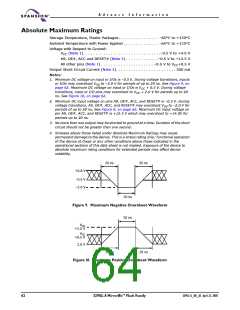
1. Minimum DC voltage on input or I/Os is –0.5 V. During voltage transitions, inputs
or I/Os may overshoot VSS to –2.0 V for periods of up to 20 ns. See Figure 9, on
page 62. Maximum DC voltage on input or I/Os is VCC + 0.5 V. During voltage
transitions, input or I/O pins may overshoot to VCC + 2.0 V for periods up to 20
ns. See Figure 10, on page 62.
2. Minimum DC input voltage on pins A9, OE#, ACC, and RESET# is –0.5 V. During
voltage transitions, A9, OE#, ACC, and RESET# may overshoot VSS to –2.0 V for
periods of up to 20 ns. See Figure 9, on page 62. Maximum DC input voltage on
pin A9, OE#, ACC, and RESET# is +12.5 V which may overshoot to +14.0V for
periods up to 20 ns.
3. No more than one output may be shorted to ground at a time. Duration of the short
circuit should not be greater than one second.
4. Stresses above those listed under Absolute Maximum Ratings may cause
permanent damage to the device. This is a stress rating only; functional operation
of the device at these or any other conditions above those indicated in the
operational sections of this data sheet is not implied. Exposure of the device to
absolute maximum rating conditions for extended periods may affect device
reliability.
20 ns
20 ns
+0.8 V
–0.5 V
–2.0 V
20 ns
Figure 9. Maximum Negative Overshoot Waveform
20 ns
VCC
+2.0 V
VCC
+0.5 V
2.0 V
20 ns
20 ns
Figure 10. Maximum Positive Overshoot Waveform
62
S29GL-A MirrorBit™ Flash Family
S29GL-A_00_A3 April 22, 2005

 SPANSION [ SPANSION ]