A d v a n c e I n f o r m a t i o n
Table of Contents
Persistent Sector Protection .......................................................................................27
Password Sector Protection ........................................................................................27
WP# Hardware Protection .........................................................................................27
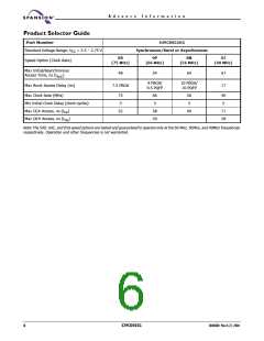
Product Selector Guide . . . . . . . . . . . . . . . . . . . . . .6
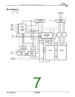
Block Diagram . . . . . . . . . . . . . . . . . . . . . . . . . . . . . 7
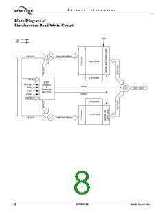
Block Diagram of
Simultaneous Read/Write Circuit . . . . . . . . . . . . . .8
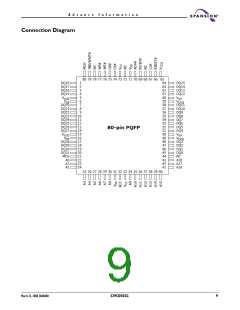
Connection Diagram . . . . . . . . . . . . . . . . . . . . . . . .9
Special Package Handling Instructions .............................................10
Pin Configuration . . . . . . . . . . . . . . . . . . . . . . . . . . 11
Logic Symbols . . . . . . . . . . . . . . . . . . . . . . . . . . . . 12
x32 Mode .................................................................................................. 12
Ordering Information . . . . . . . . . . . . . . . . . . . . . . . 13
Device Bus Operations . . . . . . . . . . . . . . . . . . . . . . 14
Table 1. Device Bus Operation ............................................14
Persistent Sector Protection ............................................................ 28
Persistent Protection Bit (PPB) ..................................................................................28
Persistent Protection Bit Lock (PPB Lock) .............................................................28
Dynamic Protection Bit (DYB) ...................................................................................28
Table 11. Sector Protection Schemes .................................. 30
Persistent Sector Protection Mode Locking Bit ......................... 30
Password Protection Mode ............................................................... 30
Password and Password Mode Locking Bit ....................................31
64-bit Password ................................................................................................................31
Write Protect (WP#) ..........................................................................32
SecSi™ (Secured Silicon) Sector Protection ..................................32
SecSi Sector Protection Bit ................................................................33
Persistent Protection Bit Lock ..........................................................33
VersatileI/O™ (V ) Control .............................................................. 15
Requirements for Reading Array Data ........................................... 15
Simultaneous Read/Write
IO
Hardware Data Protection ................................................................33
Low VCC Write Inhibit .................................................................................................. 33
Write Pulse “Glitch” Protection ................................................................................ 33
Logical Inhibit ...................................................................................................................34
Power-Up Write Inhibit ................................................................................................34
VCC and VIO Power-up And Power-down Sequencing ......................................34
Table 12. Sector Addresses for Ordering Option 00 ............... 35
Table 13. Sector Addresses for Ordering Option 01 ............... 38
Operations Overview and Restrictions .......................................... 15
Overview ............................................................................................................................15
Restrictions ........................................................................................................................15
Table 2. Bank Assignment for Boot Bank
Sector Devices .................................................................16
Simultaneous Read/Write Operations With Zero Latency .....16
Table 3. Ordering Option 00 ...............................................16
Table 4. Ordering Option 01 ...............................................16
Common Flash Memory Interface (CFI) . . . . . . . .41
Table 14. CFI Query Identification String ............................. 41
Table 15. CFI System Interface String ................................. 42
Table 16. Device Geometry Definition ................................. 43
Table 17. CFI Primary Vendor-Specific Extended Query ......... 44
Command Definitions . . . . . . . . . . . . . . . . . . . . . . 46
Reading Array Data in Non-burst Mode ...................................... 46
Reading Array Data in Burst Mode ................................................ 46
Read/Reset Command .........................................................................47
Autoselect Command ..........................................................................47
Program Command Sequence ...........................................................47
Accelerated Program Command ..................................................... 48
Writing Commands/Command Sequences ...................................16
Accelerated Program and Erase Operations ..........................................................17
Autoselect Functions ......................................................................................................17
Automatic Sleep Mode (ASM) ........................................................... 17
Standby Mode ...................................................................................................................17
RESET#: Hardware Reset Pin ............................................................18
Output Disable Mode ...........................................................................18
Autoselect Mode ...................................................................................18
Table 5. S29CD032G Autoselect Codes (High Voltage Method) 19
Asynchronous Read Operation (Non-Burst) ................................19
Figure 1. Asynchronous Read Operation............................... 20
Synchronous (Burst) Read Operation ............................................20
Unlock Bypass Command Sequence .............................................. 48
Figure 4. Program Operation.............................................. 49
Unlock Bypass Entry Command .................................................................................49
Unlock Bypass Program Command ..........................................................................50
Unlock Bypass Chip Erase Command ......................................................................50
Unlock Bypass CFI Command ....................................................................................50
Unlock Bypass Reset Command ................................................................................50
Linear Burst Read Operations ..........................................................20
Table 6. 32- Bit Linear and Burst Data Order ........................21
CE# Control in Linear Mode ......................................................................................22
ADV# Control In Linear Mode ..................................................................................22
RESET# Control in Linear Mode ...............................................................................22
OE# Control in Linear Mode .....................................................................................22
IND/WAIT# Operation in Linear Mode .................................................................22
Table 7. Valid Configuration Register Bit Definition for IND/WAIT#
22
Figure 2. End of Burst Indicator (IND/WAIT#) Timing for Linear 8-
Word Burst Operation........................................................ 23
Burst Access Timing Control ...................................................................................... 23
Initial Burst Access Delay Control ............................................................................ 23
Table 8. Burst Initial Access Delay .......................................24
Figure 3. Initial Burst Delay Control..................................... 24
Burst CLK Edge Data Delivery ...................................................................................24
Burst Data Hold Control .............................................................................................24
Asserting RESET# During A Burst Access ..............................................................24
Chip Erase Command ......................................................................... 50
Sector Erase Command .......................................................................51
Figure 5. Erase Operation.................................................. 52
Sector Erase and Program Suspend Command ...........................52
Sector Erase and Program Suspend Operation Mechanics ......53
Table 18. Allowed Operations During Erase/Program Suspend 53
Sector Erase and Program Resume Command ............................54
Configuration Register Read Command ........................................54
Configuration Register Write Command ......................................54
Common Flash Interface (CFI) Command ....................................54
SecSi Sector Entry Command ............................................................55
Password Program Command ..........................................................56
Password Verify Command ................................................................56
Password Protection Mode Locking Bit Program Command .56
Persistent Sector Protection Mode Locking Bit Program Com-
Configuration Register ........................................................................ 25
Table 9. Configuration Register Definitions ...........................25
Table 10. Configuration Register After Device Reset ...............27
Initial Access Delay Configuration .................................................. 27
Sector Protection . . . . . . . . . . . . . . . . . . . . . . . . . 27
Sector and Sector Groups ........................................................................................... 27
4
S29CD032G
30606B0 March 22, 2004

 SPANSION [ SPANSION ]