A d v a n c e I n f o r m a t i o n
General Description
The S29CD032G is a 32 Megabit, 2.5 Volt-only single power supply burst mode
flash memory device. The device can be configured for 1,048,576 double words.
The device can also be programmed in standard EPROM programmers.
To eliminate bus contention, each device has separate chip enable (CE#), write
enable (WE#) and output enable (OE#) controls. Additional control inputs are re-
quired for synchronous burst operations: Load Burst Address Valid (ADV#), and
Clock (CLK).
Each device requires only a single 2.5 or 2.6 Volt power supply (2.5 V to 2.75
V) for both read and write functions. A 12.0-volt V is not required for program
PP
or erase operations, although an acceleration pin is available if faster program-
ming performance is required.
The device is entirely command set compatible with the JEDEC single-power-
supply Flash standard. The software command set is compatible with the com-
mand sets of the 5 V Am29F and 3 V Am29LV Flash families. Commands are
written to the command register using standard microprocessor write timing.
Register contents serve as inputs to an internal state-machine that controls the
erase and programming circuitry. Write cycles also internally latch addresses and
data needed for the programming and erase operations. Reading data out of the
device is similar to reading from other Flash or EPROM devices.
The Unlock Bypass mode facilitates faster programming times by requiring only
two write cycles to program data instead of four.
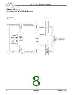
The Simultaneous Read/Write architecture provides simultaneous operation
by dividing the memory space into two banks. The device can begin programming
or erasing in one bank, and then simultaneously read from the other bank, with
zero latency. This releases the system from waiting for the completion of program
or erase operations. See Simultaneous Read/Write Operations Overview and Re-
strictions on page 13.
The device provides a 256-byte SecSi™ (Secured Silicon) Sector with an one-
time-programmable (OTP) mechanism.
In addition, the device features several levels of sector protection, which can dis-
able both the program and erase operations in certain sectors or sector groups:
Persistent Sector Protection is a command sector protection method that re-
places the old 12 V controlled protection method; Password Sector Protection
is a highly sophisticated protection method that requires a password before
changes to certain sectors or sector groups are permitted; WP# Hardware Pro-
tection prevents program or erase in the two outermost 8 Kbytes sectors of the
larger bank.
The device defaults to the Persistent Sector Protection mode. The customer must
then choose if the Standard or Password Protection method is most desirable. The
WP# Hardware Protection feature is always available, independent of the other
protection method chosen.
The VersatileI/O™ (V
) feature allows the output voltage generated on the
CCQ
device to be determined based on the V level. This feature allows this device to
IO
operate in the 1.8 V I/O environment, driving and receiving signals to and from
other 1.8 V devices on the same bus.
The host system can detect whether a program or erase operation is complete by
observing the RY/BY# pin, by reading the DQ7 (Data# Polling), or DQ6 (toggle)
2
S29CD032G
30606B0 March 22, 2004

 SPANSION [ SPANSION ]