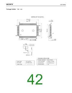
CXD1199AQ
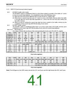
3-2-5. HINTSTS (host interrupt status) register
bit 4 : BFWRDY (buffer write ready)
The BFWRDY status is established if there is area where writing is possible in the buffer of 1 sector
or more for sound map playback. It is established in any of the following cases:
(1) When the host has set the SMEN bit (bit 5) of the HCHPCTL register high
(2) When there is sound map data area of 1 sector or more in the buffer memory (when the buffer
is not full) after the sound map data equivalent to 1 sector from the host has been written into
the buffer memory
(3) When an area for writing the sound map data has been created in the buffer memory by the
completion of the sound map ADPCM decoding of one sector
bit 3 : BFEMPT (buffer empty)
The BFEMPT status is established when there is no more sector data in the buffer memory upon
completion of the sound map ADPCM decoding of one sector for sound map playback.
bits 2 to 0 : INTSTS#2 to 0
The values of these bits are those of the corresponding bits for the sub CPU HIFCTL register.
bit7
“L”
bit6
“L”
bit5
“L”
bit4
“L”
bit3
“L”
bit2
“L”
bit1
RA1
bit1
bit1
“L”
bit0
RA0
bit0
bit0
“L”
REG
ADR
0/
ADDRESS
bit7
bit6
bit5
bit4
bit4
“L”
bit3
bit3
“L”
bit2
bit2
“L”
COMMAND 10
PARAMETER 20
HCHP CTL 30
bit7
bit6
bit5
BFRD
bit7
BFWR
bit6
SMEN
bit5
WR DATA
11
bit4
bit3
bit2
bit1
bit0
“L”
“L”
“L”
ENBF WRDY ENBF EMPT
EN INT#2 EN INT#1 EN INT#0
SMADP CLR CLRBF WRDY CLRBF EMPT
CLR INT#2 CLR INT#1 CLR INT#0
HINT MSK 21
HCLR CTL 31
CHP RST
“L”
CLR PRM
EMPHASIS
bit6
CI
ATV0
12
22
32
13
23
33
“L”
bit5
BIT LNGTH
bit4
“L”
bit3
bit3
bit3
bit3
“L”
FS
bit2
bit2
bit2
bit2
“L”
“L”
bit1
bit1
bit1
bit1
“L”
S/M
bit0
bit7
bit7
bit6
bit5
bit4
bit0
ATV1
bit7
bit6
bit5
bit4
bit0
ATV2
bit7
bit6
bit5
bit4
bit0
ATV3
“L”
“L”
CHNG ATV
“L”
ADP MUTE
ADP CTL
Host write registers
REG
HSTS
ADR
bit7
bit6
bit5
bit4
bit3
bit2
bit1
RA1
bit1
bit1
bit0
RA0
bit0
bit0
0/ BUSY STS DRQ STS RSL RRDY PRM WRDY PRM EMPT ADP BUSY
RESULT
RD DATA
1/
2/
bit7
bit7
—
bit6
bit6
—
bit5
bit5
—
bit4
bit4
bit3
bit3
bit2
bit2
HINT MSK 3/0
HINT STS 3/1
ENBF WRDY ENBF EMPT EN ENT#2 EN ENT#1 EN ENT#0
BF WRDY BF EMPT INT STS#2 INT STS#1 INT STS#0
—
—
—
Host read registers
Note) The left figures in the ADR column denote the HA1 and 0 pins and the right denote the RA1 and 0 pins.
—41—

 SONY [ SONY CORPORATION ]