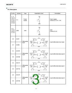
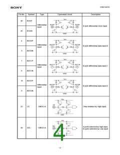
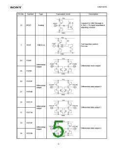
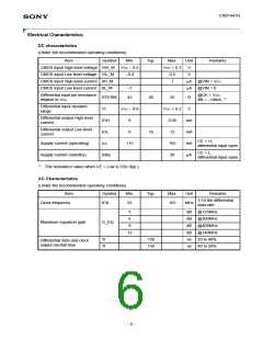
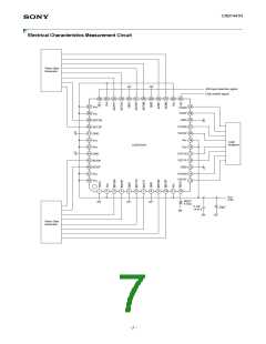
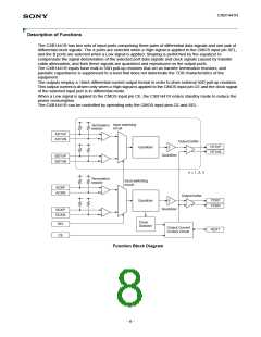
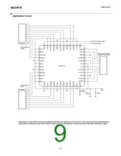
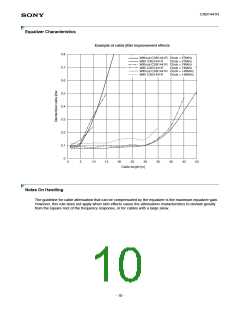
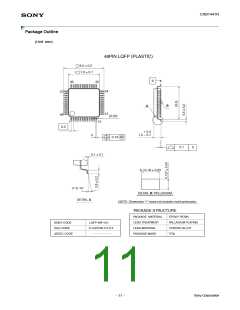
CXB1441R
Application Circuit
A/B input selection signal
Chip enable signal
Receptacle A
36 35 34 33 32 31 30 29 28 27 26 25
ESD protective
device
37
38
39
40
41
42
43
44
45
46
47
48
24
23
22
21
20
19
18
17
16
15
14
13
Vcc
YCKN
YCKP
GND
Vcc
Frame internal wiring
Cable/FPC receptacle
ADT2N
ADT2P
GND
Vcc
YDT0N
YDT0P
Vcc
CXB1441R
Vcc
Vcc
YDT1N
YDT1P
GND
GND
BCKN
BCKP
Vcc
YDT2N
YDT2P
Vcc
ESD protective
device
1
2
3
4
5
6
7
8
9
10 11 12
Vcc
3.3V
Receptacle B
REXT
4.7kΩ
0.1µF
×4 to 5
33µF
Application circuits shown are typical examples illustrating the operation of the devices. Sony cannot assume responsibility for
any problems arising out of the use of these circuits or for any infringement of third party patent and other right due to same.
- 9 -

 SONY [ SONY CORPORATION ]