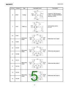
CXB1441R
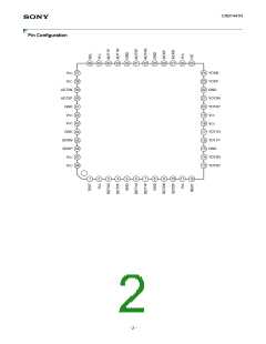
Pin Description
Pin No.
Symbol
Type
Equivalent circuit
Description
Vcc
2, 11,
18, 19,
26, 35,
37, 38,
42, 43,
47, 48
Power
supply
Power supply.
Connect to 3.3V ± 5%.
VCC
GND
Vcc
5, 8,
15, 22,
29, 32,
41, 44
GND.
Connect to 0V.
GND
GND
GND
Vcc
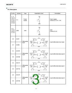
28
27
31
30
34
33
40
39
ACKP
ACKP
28
ACKN
27
Differential
input
A port differential clock input.
A port differential data input 0.
A port differential data input 1.
A port differential data input 2.
ACKN
GND
Vcc
ADT0P
ADT0N
ADT1P
ADT1N
ADT2P
ADT2N
ADT0P
31
ADT0N
30
Differential
input
GND
Vcc
ADT1P
34
ADT1N
33
Differential
input
GND
Vcc
ADT2P
40
ADT2N
39
Differential
input
GND
- 3 -

 SONY [ SONY CORPORATION ]