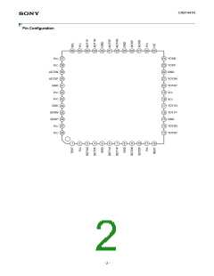
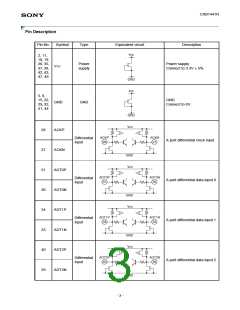
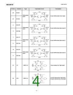
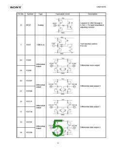
CXB1441R
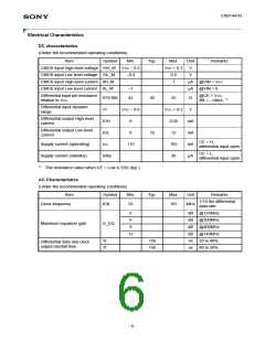
Electrical Characteristics
DC characteristics
(Under the recommended operating conditions)
Item
Symbol
Min.
VCC – 0.5
–0.3
Typ.
Max.
VCC + 0.3
0.5
Unit
V
Remarks
CMOS input High level voltage VIH_M
CMOS input Low level voltage VIL_M
CMOS input High level current IIH_M
CMOS input Low level current IIL_M
V
1
µA @VIN = VCC
µA @VIN = 0
–1
45
Differential input pin resistance
RTERM
@CE = VCC,
Ω
50
10
55
VCC + 0.2
0.05
12
relative to VCC
IIN = –10mA, *1
Differential input dynamic
VI
VCC – 0.8
V
range
Differential output High level
IOH
0
8
mA
mA
current
Differential output Low level
IOL
current
CE = H,
mA
Supply current (operating)
Supply current (standby)
ICC
110
165
differential input open
CE = L,
Istby
30
µA
differential input open
*1
The resistance value when CE = Low is 55Ω (typ.).
AC Characteristics
(Under the recommended operating conditions)
Item
Clock frequency
Symbol
fCK
Min.
25
Typ.
Max.
165
Unit
Remarks
1/10 the differential
data rate
MHz
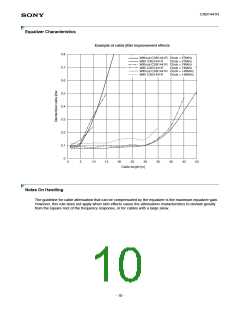
5
6
dB @125MHz
dB @200MHz
dB @400MHz
dB @740MHz
ns 20 to 80%
ns 80 to 20%
Maximum equalizer gain
G_EQ
9
12
Tr
Tf
150
150
Differential data and clock
output rise/fall time
- 6 -

 SONY [ SONY CORPORATION ]