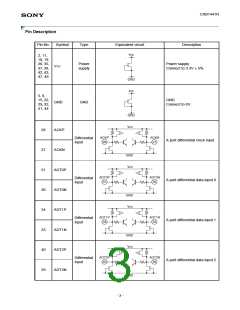
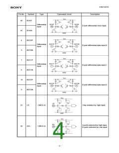
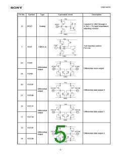
CXB1441R
Description of Functions
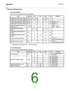
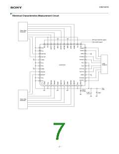
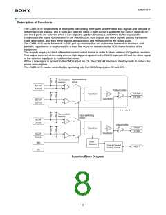
The CXB1441R has two sets of input ports comprising three pairs of differential data signals and one pair of
differential clock signals. The A ports are selected when a High signal is applied to the CMOS input pin SEL,
and the B ports are selected when a Low signal is applied. Shaping is performed by the equalizer to
compensate the signal deterioration of the selected port data signals and clock signals caused by transfer
cable attenuation, and then these signals are quantized and reproduced on the output ports.
The CXB1441R inputs have built-in 50Ω pull-up resistors that act as transfer termination resistors, and
parasitic capacitance is suppressed to a level that does not deteriorate the TDR characteristics of the
equipment.
The outputs employ a 10mA differential current output format in order to drive external 50Ω pull-up resistors.
This output current is driven only when a High signal is applied to the CMOS input pin CE and the clock signal
of the selected input port is in differential mode.
When a Low signal is applied to the CMOS input pin CE, the CXB1441R enters standby mode to reduce the
power consumption.
The CXB1441R can be controlled by operating only the CMOS input pins CE and SEL.
Input switching
circuit
Termination
resistor
ADTnP
ADTnN
Output buffer
YDTnP
YDTnN
Equalizer
Quantizer
BDTnP
BDTnN
n = 1, 2, 3
Termination
resistor
Input switching
circuit
ACKP
ACKN
Output buffer
YCKP
YCKN
Equalizer
Quantizer
BCKP
BCKN
Clock
Detector
SEL
CE
Output Current
Control Circuit
REXT
Function Block Diagram
- 8 -

 SONY [ SONY CORPORATION ]