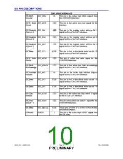
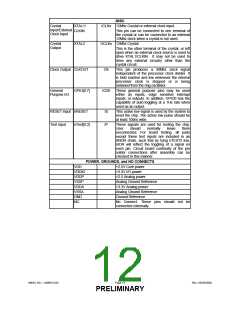
MISC
Crystal
Input/External
Clock Input
XTAL1/
CLKIN
ICLKx 12Mhz Crystal or external clock input.
This pin can be connected to one terminal of
the crystal or can be connected to an external
12Mhz clock when a crystal is not used.
Crystal
Output
XTAL2
OCLKx 12Mhz Crystal
This is the other terminal of the crystal, or left
open when an external clock source is used to
drive XTAL1/CLKIN. It may not be used to
drive any external circuitry other than the
crystal circuit.
Clock Output CLKOUT
O8
This pin produces a 30Mhz clock signal
independent of the processor clock divider. It
is held inactive and low whenever the internal
processor clock is stopped or is being
obtained from the ring oscillator.
General
Purpose I/O
GPIO[0:7]
IO20
These general purpose pins may be used
either as inputs, edge sensitive interrupt
inputs, or outputs. In addition, GPIO0 has the
capability of auto-toggling at a 1Hz rate when
used as an output.
RESET input nRESET
IS
IP
This active low signal is used by the system to
reset the chip. The active low pulse should be
at least 100ns wide.
Test input
nTest[0:2}
These signals are used for testing the chip.
User
should
normally
leave
them
unconnected. For board testing, all pads
except these test inputs are included in an
XNOR chain, such that by tying nTEST2 low,
nIOR will reflect the toggling of a signal on
each pin. Circuit board continuity of the pin
solder connections after assembly can be
checked in this manner
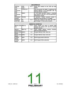
POWER, GROUNDS, and NO CONNECTS
+2.5V Core power
VDD
VDDIO
VDDP
VSSP
VDDA
VSSA
GND
+3.3V I/O power
+2.5 Analog power
Analog Ground Reference
+3.3V Analog power
Analog Ground Reference
Ground Reference
NC
No Connect. These pins should not be
connected externally.
SMSC DS – USB97C201
Page 12
Rev. 03/25/2002
PRELIMINARY

 SMSC [ SMSC CORPORATION ]