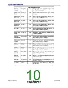
5.0 PIN DESCRIPTIONS
DISK DRIVE INTERFACE
IDE DMA
Request
IDE_DRQ
IS
This pin is the active high DMA request from
the ATA/ATAPI interface.
IDE IO Read IDE_nIOR
Strobe
O20
O20
O20
O20
IO20
O20
O20
IS
This pin is the active low read signal for the
interface.
IDE Register IDE_SA1
Address 1
This pin is the register select address bit 1
signal for the ATA/ATAPI interface.
IDE Register IDE_SA0
Address 0
This pin is the register select address bit 0
signal for the ATA/ATAPI interface.
IDE Register IDE_SA2
Address 2
This pin is the register select address bit 2
signal for the ATA/ATAPI interface.
IDE Data
IDE_D15
This pin is the bi-directional data bus bit 15
signal for the ATA/ATAPI interface.
IDE IO Write IDE_nIOW
Strobe
This pin is active low write signal for the
ATA/ATAPI interface.
IDE DMA
IDE_nDACK
This pin is the active low DMA acknowledge
signal for the ATA/ATAPI interface.
Acknowledge
IDE Interrupt IDE_IRQ
Request
This pin is the active high interrupt request
signal for the ATA/ATAPI interface.
IDE Data
IDE Data
IDE_D13
IDE_D14
IDE_nCS0
IDE_nCS1
IO20
IO20
O20
O20
This pin is the bi-directional data bus bit 13
signal for the ATA/ATAPI interface.
This pin is the bi-directional data bus bit 14
signal for the ATA/ATAPI interface.
.
IDE Chip
Select 0
This pin is the active low chip select 0 signal
for the ATA/ATAPI interface.
IDE Chip
Select 1 0
This pin is the active low select 1 signal for the
ATA/ATAPI interface.
IDE Data
IO Ready
IDE_D[0:12]
IORDY
IO20
I
These pins are bits 0-12 of the ATA/ATAPI bi-
directional data bus.
This pin is the active high IORDY signal from
the IDE drive.
SMSC DS – USB97C201
Page 10
Rev. 03/25/2002
PRELIMINARY

 SMSC [ SMSC CORPORATION ]