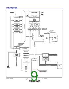
4.0 BLOCK DIAGRAM
Auto address generators
512 Bytes EP2 TX/RX Buffer B
512 Bytes EP2 TX/RX Buffer A
1.25KB
SRAM
Address
Address
Address
64 Bytes EP1RX
64 Bytes EP1TX
64 Bytes EP0RX
64 Bytes EP0TX
EP0TX_BC
EP0RX_BC
EP1TX_BC
EP1RX_BC
Address
Address
32 Bit
60MHz
Latch phase 1
Latch phase 2
Future phase 3
Latch phase 0
RAMWR_A/B
RAMRD_A/B
Address
Address
Granted SRAM access
during Phase 2
Data @ 32 bit
15MHz
ATA/ATAPI
Drive
ATA-66
Interface
Granted SRAM access
during Phase 0
SIE
32 bit 15MHz Data Buss
( Serial Interface Engine )
SIE Control Regs
USB 2.0 PHY
( Transceiver )
GPIO
8 pins
Configuration and Control
768 Byte
Program/Scratchpad
SRAM
Clock Generation
Osc
Interrupt Controller
Program Memory/ IO
Bus
MEM/IO Bus
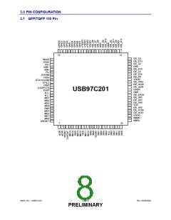
29pins
OPTIONAL
External PHY
FAST 8051
CPU CORE
CLOCKOUT
12 MHz
Granted SRAM access during Phase 1
SMSC DS – USB97C201
Page 9
Rev. 03/25/2002
PRELIMINARY

 SMSC [ SMSC CORPORATION ]