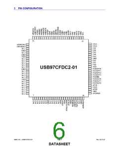
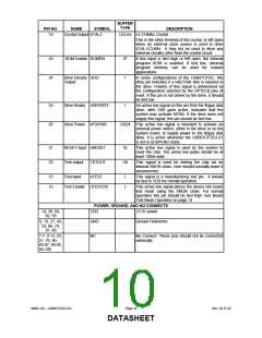
BUFFER
TYPE
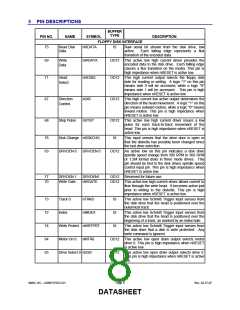
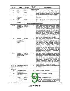
PIN NO.
NAME
SYMBOL
DESCRIPTION
18
Crystal Output XTAL2
OCLKx 14.318Mhz Crystal
This is the other terminal of the crystal, or left open
when an external clock source is used to drive
XTAL1/CLKIN. It may not be used to drive any
external circuitry other than the crystal circuit.
20
24
ROM Enable ROMEN
IP
I
If this input is tied high or left open, the internal
program ROM is enabled. If tied low, external
program memory can be used for custom
applications.
Drive Density HDO
Output
In some configurations of the USB97CFDC, this
drive pin indicates if a 640/720K disk is inserted in
the drive. Polarity of this signal is determined by
the configuration selected by the OPT[3:0] pins at
reset. If this pin is not driven by the drive, it should
be tied low.
25
26
Drive Ready nDRVRDY
Drive Power nFDPWR
I
An active low signal on this pin from the floppy disk
drive, after DS0 goes active, indicates that the
system may activate MTR0. If the drive does not
supply this signal, this pin should be tied low.
OD24 This active low signal is intended to activate an
external power switch, either in the drive or on the
system board, to supply power to the floppy disk
drive. It is active whenever the USB97CFDC2-01
is not in SUSPEND mode.
21
22
RESET input nRESET
IS
This active low signal is used by the system to
reset the chip. The active low pulse should be at
least 100ns wide.
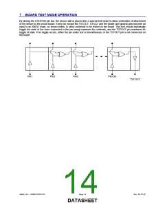
Test output
Test input
TSTOUT
nTEST
O8
This signal is used for testing the chip via an
internal XNOR chain. User should normally leave it
unconnected.
15
16
I
I
This signal is a manufacturing test pin. It should
be tied to VDD for normal operation.
Test Enable nTESTEN
This active low signal places the device into board
test mode using the XNOR chain. For normal
operation this pin should be tied high. See Board
Test Mode Operation on page 14
POWER, GROUND, AND NO CONNECTS
14, 39, 60,
82, 93
VDD
+3.3V power
8, 19, 27, 43,
52, 66, 79,
81, 88
GND
NC
Ground Reference
1-7, 9-13, 23,
51, 78, 80,
83-87, 89-92,
94-100
No Connect. These pins should not be connected
externally.
SMSC DS – USB97CFDC2-01
Page 10
Rev. 02-27-07
DATASHEET

 SMSC [ SMSC CORPORATION ]