Hi-Speed USB Transceiver with 1.8V-3.3V ULPI Interface - 13MHz Reference Clock
Table 1 USB3318 Pin Description (continued)
Output,
CMOS
N/A
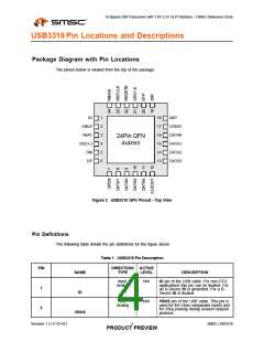
Controls the direction of the data bus.
When the PHY has data to transfer to the
Link, it drives DIR high to take ownership
of the bus. When the PHY has no data to
transfer it drives DIR low and monitors
the bus for commands from the Link.
19
DIR
Input,
CMOS
High
The Link asserts STP for one clock cycle
to stop the data stream currently on the
bus. If the Link is sending data to the
PHY, STP indicates the last byte of data
was on the bus in the previous cycle.
20
21
STP
Power
N/A
N/A
External 1.8V Supply input pin. This pad
needs to be bypassed with a 0.1uF
capacitor to ground, placed as close as
possible to the USB3318.
VDD1.8
Input,
CMOS,
When low, the part is suspended with all
of the I/O tri-stated. When high the
USB3318 will operate as a normal ULPI
device.
22
23
RESETB
REFCLK
Input,
CMOS
N/A
N/A
13MHz Reference Clock input.
Analog,
CMOS
Rbias pin. This pin requires an 8.06kΩ
(±1%) resistor to ground, placed as close
as possible to the USB3318.
24
RBIAS
GND
Ground
N/A
Ground.
QFN only: The flag should be connected
to the ground plane with a via array
under the exposed flag. This is the main
ground for the IC.
FLAG
Revision 1.3 (11-02-07)
6
SMSC USB3318
PRODUCT PREVIEW

 SMSC [ SMSC CORPORATION ]