Hi-Speed USB Transceiver with 1.8V-3.3V ULPI Interface - 13MHz Reference Clock
General Description
The USB3318 is a highly integrated Hi-Speed USB 2.0 Transceiver (PHY) that supports systems
architectures based on a 13MHz reference clock. It is designed to be used in both commercial and
industrial temperature applications.
The USB3318 meets all of the electrical requirements to be used as a Hi-Speed USB Host, Device,
or an On-the-Go (OTG) device. In addition to the supporting USB signaling the USB3318 also provides
USB UART mode
USB3318 uses the industry standard UTMI+ Low Pin Interface (ULPI) to connect the USB PHY to the
Link. The industry standard ULPI interface uses a method of in-band signaling and status byte transfers
between the Link and PHY, to facilitate a USB session. By using in-band signaling and status byte
transfers the ULPI interface requires only 12 pins.
The USB3318 uses SMSC’s “wrapper-less” technology to implement the ULPI interface. This “wrapper-
less” technology allows the PHY to achieve a low latency transmit and receive time. SMSC’s low
latency transceiver allows an existing UTMI Link to be reused by adding a UTMI to ULPI bridge. By
adding a bridge to the ASIC the existing and proven UTMI Link IP can be reused.
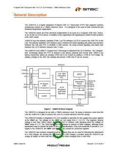
REFCLK
CPEN
VBUS
ID
Low Jitter
Integrated
PLL
OTG
RBIAS
BIAS
RESETB
VBAT
VDD33
VDD18
Integrated
Power
Management
Hi-Speed
USB
Transceiver
DP
DM
ULPI
VDDIO
Registers
and State
Machine
STP
NXT
DIR
CLKOUT
ULPI Interface
DATA[7:0]
Carkit
Figure 1 USB3318 Block Diagram
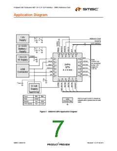
The USB3318 is designed to run with a 13MHz reference clock. By using a reference clock from the
Link the USB3318 is able to remove the cost of a crystal reference from the design.
The USB3318 includes a integrated 3.3V LDO regulator to generate its own supply from power applied
at the VBAT pin. The voltage on the VBAT pin can range from 3.1 to 5.5V. The regulator dropout
voltage is less than 100mV which allows the PHY to continue USB signaling when the voltage on
VBAT drops to 3.1V. The USB transceiver will continue to operate at lower voltages, although some
parameters may be outside the limits of the USB specifications. If the user would like to provide a 3.3V
supply to the USB3318, the VBAT and VDD3.3 pins should be connected together.
The USB3318 also includes integrated pull-up resistors that can be used for detecting the attachment
of a USB Charger. By sensing the attachment to a USB Charger, a product using the USB3318 can
charge its battery at more than the 500mA allowed when charging from a USB Host.
SMSC USB3318
3
Revision 1.3 (11-02-07)
PRODUCT PREVIEW

 SMSC [ SMSC CORPORATION ]