Hi-Speed USB Transceiver with 1.8V-3.3V ULPI Interface - 13MHz Reference Clock
Table 1 USB3318 Pin Description (continued)
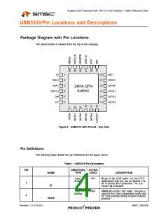
Power
N/A
Regulator input. The regulator supply can
be from 5.5V to 3.1V.
3
VBAT
Power
N/A
3.3V Regulator Output. A 2.2uF (<1 ohm
ESR) bypass capacitor to ground is
required for regulator stability. The
bypass capacitor should be placed as
close as possible to the USB3318.
4
5
6
VDD3.3
DM
I/O,
N/A
N/A
D- pin of the USB cable.
Analog
I/O,
Analog
D+ pin of the USB cable.
DP
Output,
CMOS
High
External 5 volt supply enable. This pin is
used to enable the external Vbus power
supply. The CPEN pin is low on POR.
This pad uses VDD3.3 logic level.
7
8
CPEN
I/O,
N/A
N/A
N/A
N/A
N/A
ULPI bi-directional data bus. DATA[7] is
the MSB.
CMOS
DATA[7]
DATA[6]
DATA[5
DATA[4]
I/O,
CMOS
9
ULPI bi-directional data bus.
ULPI bi-directional data bus.
ULPI bi-directional data bus.
I/O,
CMOS
10
11
I/O,
CMOS
Output,
CMOS
60MHz reference clock output. All ULPI
signals are driven synchronous to the
rising edge of this clock.
12
13
14
15
16
CLKOUT
DATA[3]
DATA[2]
DATA[1]
DATA[0]
I/O,
CMOS
N/A
N/A
N/A
N/A
N/A
ULPI bi-directional data bus.
ULPI bi-directional data bus.
ULPI bi-directional data bus.
I/O,
CMOS
I/O,
CMOS
I/O,
CMOS
ULPI bi-directional data bus. DATA[0] is
the LSB.
Power
1.8V to 3.3V ULPI interface supply
voltage. This voltage sets the value of
VOH for the ULPI interface.
17
VDDIO
Output,
CMOS
High
The PHY asserts NXT to throttle the data.
When the Link is sending data to the
PHY, NXT indicates when the current
byte has been accepted by the PHY. The
Link places the next byte on the data bus
in the following clock cycle.
18
NXT
SMSC USB3318
5
Revision 1.3 (11-02-07)
PRODUCT PREVIEW

 SMSC [ SMSC CORPORATION ]