Hi-Speed USB Transceiver with 1.8V-3.3V ULPI Interface - 13MHz Reference Clock
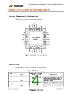
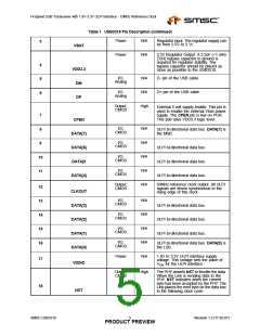
USB3318 Pin Locations and Descriptions
Package Diagram with Pin Locations
The pinout below is viewed from the top of the package.
ID
VBUS
VBAT
VDD3.3
DM
1
2
3
4
5
6
18
17
16
15
14
13
NXT
VDDIO
DATA0
DATA1
DATA2
DATA3
24Pin QFN
4x4mm
DP
Figure 2 USB3318 QFN Pinout - Top View
Pin Definitions
The following table details the pin definitions for the figure above.
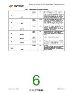
Table 1 USB3318 Pin Description
DIRECTION/ ACTIVE
PIN
1
NAME
ID
TYPE
LEVEL
DESCRIPTION
Input,
Analog
N/A
ID pin of the USB cable. For non-OTG
applications this pin can be floated. For
an A-Device ID is grounded. For a B-
Device ID is floated.
I/O,
Analog
N/A
VBUS pin of the USB cable. This pin is
used for the Vbus comparator inputs and
for Vbus pulsing during session request
protocol.
2
VBUS
Revision 1.3 (11-02-07)
4
SMSC USB3318
PRODUCT PREVIEW

 SMSC [ SMSC CORPORATION ]