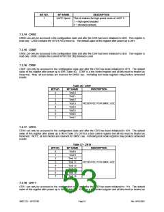
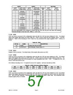
UART1
UART2
IRQ PINS
UART1
UART1 IRQ
UART2
OUT2 bit
UART2 IRQ
Share
IRQ
UART1
UART2
Output State
Output State
OUT2 bit
Pin State
Pin State
1
1
1
0
1
1
0
0
1
1
1
1
asserted
de-asserted
de-asserted
Z
asserted
de-asserted
Z
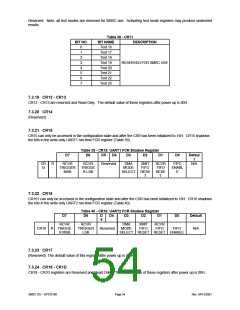
1
1
1
0
0
0
1
1
1
1
1
1
de-asserted
asserted
de-asserted
Z
No
No
No
1
0
0
Z
1
0
1
0
1
1
1
0
0
1
0
Z
Z
Z
Z
Z
Z
Z
Z
Z
Yes
Yes
Yes
Yes
Yes
Yes
Yes
Yes
Yes
Z
Z
asserted
de-asserted
asserted
de-asserted
asserted
de-asserted
Z
asserted
asserted
de-asserted
de-asserted
It is the responsibility of the software to ensure that two IRQ’s are not set to the same IRQ number.
Potential damage to chip may result. Note: Z = Don’t Care.
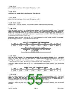
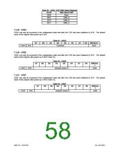
7.3.35 CR29
CR29 can only be accessed in the configuration state and after the CSR has been initialized to 29H. The default
value of this register after power up is 00H (Table 48). CR29 is used to select the IRQ mapping (bits 0 - 3) for the
IRQIN pin. Refer to IRQ encoding for CR27 (Table 46). Any unselected IRQ output (registers CR27 - CR29) is in
tristate.
Table 48 - CR29
BIT NO.
0-3
NAME
IRQIN
RESERVED
DESCRIPTION
Selects the IRQ for IRQIN
Not Writeable, Reads Return “0”
4-7
7.3.36 CR2A
Register CR2A is reserved. The default value of this register after power up is 00H.
7.3.37 CR2B
CR2B can only be accessed in the configuration state and after the CSR has been initialized to 2BH. The default
value of this register after power up is 00H (Table 49). CR2B is used to set the SCE base address ADR[10:3]. The
SCE base address can be set to 224 locations on 8-byte boundaries from 100H - 7F8H. To disable the SCE, set
ADR10, ADR9 and ADR8 to zero.
SCE Address Decoding: nCS = ’0’ required to access SCE registers. A[2:0] are decoded as XXXb.
Table 49 - CR2B: SCE Base Address Register
DB7
ADR10
DB6
ADR9
DB5
DB4
DB3
DB2
DB1
ADR4
DB0
ADR3
ADR8
ADR7
ADR6
ADR5
7.3.38 CR2C
CR2C can only be accessed in the configuration state and after the CSR has been initialized to 2CH. The default
value of this register after power up is 00H (Table 50). Bits D[3:0] of this register are used to select the DMA for the
SCE. Bits D[7:4] are Reserved. Reserved bits cannot be written and return 0 when read. Any unselected DMA
Request output (DRQ) is in tristate.
SMSC DS – SP37E760
Page 57
Rev. 04/13/2001

 SMSC [ SMSC CORPORATION ]