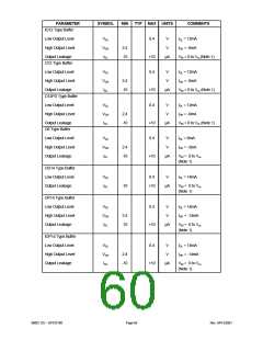
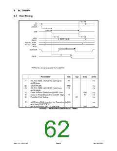
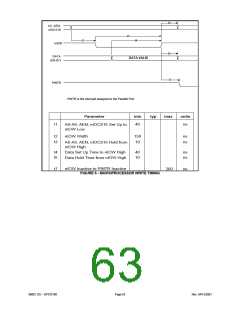
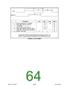
PARAMETER
O4 Type Buffer
SYMBOL
MIN
TYP MAX UNITS
COMMENTS
Low Output Level
High Output Level
Output Leakage
VOL
VOH
IOL
0.4
V
V
I
OL = 4mA
OH = -2mA
IN = 0 to Vcc
2.4
-10
I
+10
µA
V
(Note 1)
OD12 Type Buffer
Low Output Level
Output Leakage
VOL
IOL
0.4
V
I
OL = 12 mA
-10
+10
µA
VIN = 0 to Vcc
(Note 1)
20
Supply Current Active
ICC
15
mA
All outputs open.
100
±10
Supply Current Standby
ICSBY
IIL
µA
µA
Note 3
ChiProtect
Chip in circuit:
(SLCT, PE, BUSY, nACK,
nERROR)
V
CC = 0V
V
IN = 5.5V Max.
Backdrive Protect
IIL
±10
µA
Chip in circuit:
(nSLCTIN, nINIT, nAUTOFD,
nSTROBE, PD[7:0])
V
CC = 0V
VIN = 5.5V Max.
Note 1: Output leakage is measured with the current pins in high impedance as defined by the PWRGD pin.
Note 2: Output leakage is measured with the low driving output off, either for a high level output or a high impedance
state defined by PWRGD.
Note 3: Defined by the device configuration with the PWRGD input low.
CAPACITANCE TA = 25°C; fc = 1MHz; VCC = 3.3V
Table 55 - Clock Pin Loading
PARAMETER
SYMBOL
LIMITS
TYP
UNIT
TEST CONDITION
MIN
MAX
Clock Input Capacitance
CIN
20
pF
All pins except pin
under test tied to AC
ground
Input Capacitance
Output Capacitance
CIN
COUT
10
20
pF
pF
Table 56 - Capacitive Loading per Output Pin
SIGNAL NAME
SD[0:7]
IOCHRDY
IRQs
DRQs
TXD
nRTS
TOTAL CAPACITANCE (pF)
240
240
120
120
100
100
100
240
240
240
nDTR
PD[7:0]
nSLCTIN
nINIT
SMSC DS – SP37E760
Page 61
Rev. 04/13/2001

 SMSC [ SMSC CORPORATION ]