Advanced I/O Controller with Motherboard GLUE Logic
Datasheet
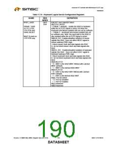
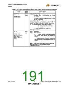
Table 11.14 – Power Control/Runtime Register Block Logical Device Configuration Registers
REG
NAME
DEFINITION
INDEX
CLOCKI32
0xF0
Bit[0] (CLK32_PRSN)
(R/W)
0=32kHz clock is connected to the CLKI32
Default = 0x00
on VTR POR
pin (default)
1=32kHz clock is not connected to the CLKI32
pin (pin is grounded)
Bit[1] SPEKEY_EN. This bit is used to turn the logic for
the “wake on specific key” feature on and off. It will
disable the 32kHz clock input to the logic when turned
off. The logic will draw no power when disabled.
0= “Wake on specific key” logic is
on (default)
1= “Wake on specific key” logic is off
Bits[7:2] are reserved
Bit[7:1] Reserved
INT_G
0xF1
R/W
Bit[0]
INT_G Enable
Default = 0x00
on VCC POR, VTR
POR, HARD
0 =
Disable Interrupt Generating Registers
(INT_GENx) from affecting the serial IRQ
stream
RESET and SOFT
RESET
1 = Enable Interrupt Generating Registers to
drive one or more frames low in the SER IRQ
stream
Note: See Power Control Block runtime registers at
offset 0x1B and 0x1C for configuring Interrupt
Generating Registers.
SMSC LPC47M182
191
Revision 1.8 SMSC/Non-SMSC Register Sets (02-24-05)
DATASHEET

 SMSC [ SMSC CORPORATION ]