Advanced I/O Controller with Motherboard GLUE Logic
Datasheet
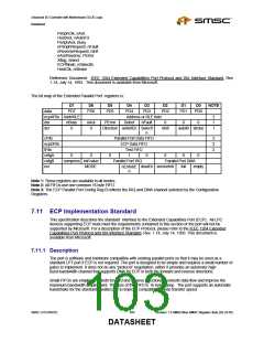
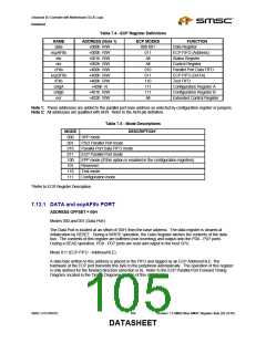
Table 7.4 - ECP Register Definitions
NAME
data
ecpAFifo
dsr
dcr
cFifo
ecpDFifo
tFifo
cnfgA
cnfgB
ecr
ADDRESS (Note 1)
+000h R/W
+000h R/W
+001h R/W
+002h R/W
+400h R/W
+400h R/W
+400h R/W
+400h R
ECP MODES
FUNCTION
Data Register
ECP FIFO (Address)
Status Register
000-001
011
All
All
Control Register
010
011
110
111
111
All
Parallel Port Data FIFO
ECP FIFO (DATA)
Test FIFO
Configuration Register A
Configuration Register B
Extended Control Register
+401h R/W
+402h R/W
Note 1: These addresses are added to the parallel port base address as selected by configuration register or jumpers.
Note 2: All addresses are qualified with AEN. Refer to the AEN pin definition.
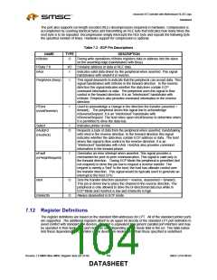
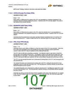
Table 7.5 - Mode Descriptions
MODE
000
001
010
011
100
101
110
111
DESCRIPTION*
SPP mode
PS/2 Parallel Port mode
Parallel Port Data FIFO mode
ECP Parallel Port mode
EPP mode (If this option is enabled in the configuration registers)
Reserved
Test mode
Configuration mode
*Refer to ECR Register Description
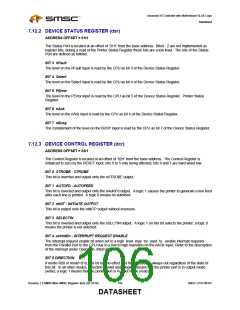
7.12.1 DATA and ecpAFifo PORT
ADDRESS OFFSET = 00H
Modes 000 and 001 (Data Port)
The Data Port is located at an offset of ‘00H’ from the base address. The data register is cleared at
initialization by RESET. During a WRITE operation, the Data Register latches the contents of the data
bus. The contents of this register are buffered (non inverting) and output onto the PD0 - PD7 ports.
During a READ operation, PD0 - PD7 ports are read and output to the host CPU.
Mode 011 (ECP FIFO - Address/RLE)
A data byte written to this address is placed in the FIFO and tagged as an ECP Address/RLE. The
hardware at the ECP port transmits this byte to the peripheral automatically. The operation of this register
is only defined for the forward direction (direction is 0). Refer to the ECP Parallel Port Forward Timing
Diagram, located in the Timing Diagrams section of this datasheet .
SMSC LPC47M182
105
Revision 1.8 SMSC/Non-SMSC Register Sets (02-24-05)
DATASHEET

 SMSC [ SMSC CORPORATION ]