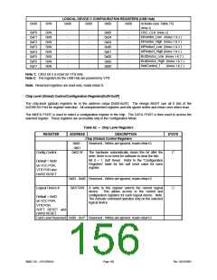
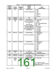
REGISTER
ADDRESS
DESCRIPTION
Chip Level, SMSC Defined
STATE
Device ID -
Hard wired
0x20 R
A
read only register which provides device
C
identification. Bits[7:0] = 0x5F when read.
Default = 0x5F
on VCC POR,
VTR POR,
SOFT RESET and
HARD RESET
Device Rev
0x21 R
A read only register which provides device revision
information. Bits[7:0] = current revision when read.
C
C
Hard wired
= Current Revision
PowerControl
0x22 R/W Bit[0] FDC Power
Bit[1] Reserved
Default = 0x00
on VCC POR,
VTR POR,
Bit[2] Game Port Power
Bit[3] Parallel Port Power
Bit[4] Serial Port 1 Power
Bit[5] Serial Port 2 Power (Note 1)
Bit[6] Serial Port 3 Power
Bit[7] Reserved
SOFT RESET and
HARD RESET
0: Power Off or Disabled
1: Power On or Enabled
Power Mgmt
0x23 R/W Bit[0] FDC (see Note in the “FDC Power
C
Management” section.)
Bit[1] Reserved
Bit[2] Reserved
Default = 0x00
on VCC POR,
VTR POR and
HARD RESET
Bit[3] Parallel Port
Bit[4] Serial Port 1
Bit[5] Serial Port 2
Bit[6] Serial Port 3
Bit[7] Reserved (read as 0)
For each bit above (except Reserved)
= 0
= 1
Intelligent Pwr Mgmt off
Intelligent Pwr Mgmt on
OSC
0x24 R/W Bit[0] Reserved
C
Bit [1] PLL Control
Default = 0x44, on
VCC POR,
VTR POR and
HARD RESET
= 0
= 1
PLL is on (backward Compatible)
PLL is off
Bits[3:2] OSC
= 01
= 10
= 00
= 11
Osc is on, BRG clock is on.
Same as above (01) case.
Osc is on, BRG Clock Enabled.
Osc is off, BRG clock is disabled.
Bit [5:4] Reserved, set to zero
Bit [6] 16-Bit Address Qualification
= 0
= 1
12-Bit Address Qualification
16-Bit Address Qualification
Note: For normal operation, bit 6 should be set.
Bit[7] Reserved
SMSC DS – LPC47M14X
Page 157
Rev. 03/19/2001

 SMSC [ SMSC CORPORATION ]