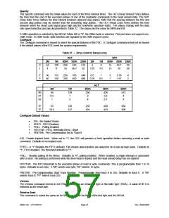
The following section describes the operation of the registers.
RECEIVE BUFFER REGISTER (RB)
Address Offset = 0H, DLAB = 0, READ ONLY
This register holds the received incoming data byte. Bit 0 is the least significant bit, which is transmitted and received
first. Received data is double buffered; this uses an additional shift register to receive the serial data stream and convert
it to a parallel 8 bit word which is transferred to the Receive Buffer register. The shift register is not accessible.
TRANSMIT BUFFER REGISTER (TB)
Address Offset = 0H, DLAB = 0, WRITE ONLY
This register contains the data byte to be transmitted. The transmit buffer is double buffered, utilizing an additional shift
register (not accessible) to convert the 8 bit data word to a serial format. This shift register is loaded from the Transmit
Buffer when the transmission of the previous byte is complete.
INTERRUPT ENABLE REGISTER (IER)
Address Offset = 1H, DLAB = 0, READ/WRITE
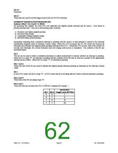
The lower four bits of this register control the enables of the five interrupt sources of the Serial Port interrupt. It is
possible to totally disable the interrupt system by resetting bits 0 through 3 of this register. Similarly, setting the
appropriate bits of this register to a high, selected interrupts can be enabled. Disabling the interrupt system inhibits the
Interrupt Identification Register and disables any Serial Port interrupt out of the LPC47M14x. All other system functions
operate in their normal manner, including the Line Status and MODEM Status Registers. The contents of the Interrupt
Enable Register are described below.
Bit 0
This bit enables the Received Data Available Interrupt (and timeout interrupts in the FIFO mode) when set to logic "1".
Bit 1
This bit enables the Transmitter Holding Register Empty Interrupt when set to logic "1".
Bit 2
This bit enables the Received Line Status Interrupt when set to logic "1". The error sources causing the interrupt are
Overrun, Parity, Framing and Break. The Line Status Register must be read to determine the source.
Bit 3
This bit enables the MODEM Status Interrupt when set to logic "1". This is caused when one of the Modem Status
Register bits changes state.
Bits 4 through 7
These bits are always logic "0".
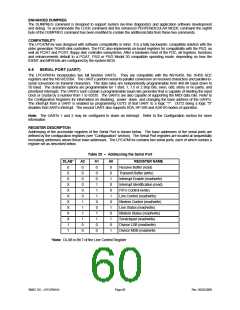
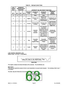
FIFO CONTROL REGISTER (FCR)
Address Offset = 2H, DLAB = X, WRITE
This is a write only register at the same location as the IIR. This register is used to enable and clear the FIFOs, set the
RCVR FIFO trigger level. Note: DMA is not supported. The UART1 and UART2 FCR’s are shadowed in the UART1
FIFO Control Shadow Register (runtime register at offset 0x20) and UART2 FIFO Control Shadow Register (runtime
register at offset 0x21).
Bit 0
Setting this bit to a logic "1" enables both the XMIT and RCVR FIFOs. Clearing this bit to a logic "0" disables both the
XMIT and RCVR FIFOs and clears all bytes from both FIFOs. When changing from FIFO Mode to non-FIFO (16450)
mode, data is automatically cleared from the FIFOs. This bit must be a 1 when other bits in this register are written to or
they will not be properly programmed.
Bit 1
Setting this bit to a logic "1" clears all bytes in the RCVR FIFO and resets its counter logic to 0. The shift register is not
cleared. This bit is self-clearing.
Bit 2
Setting this bit to a logic "1" clears all bytes in the XMIT FIFO and resets its counter logic to 0. The shift register is not
cleared. This bit is self-clearing.
Bit 3
Writing to this bit has no effect on the operation of the UART. The RXRDY and TXRDY pins are not available on this
chip.
SMSC DS – LPC47M14X
Page 61
Rev. 05/02/2000

 SMSC [ SMSC CORPORATION ]