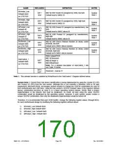
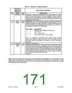
Table 76 – HubControl_1 Register Definition
HubControl_1
RESET=0x00
INDEX=0xF7
NAME
HUB CONTROL REGISTER 1
DESCRIPTION
NHubReset – When this bit is asserted (0), the hub controller is in a reset
state. The hub will not respond to any enumeration or device requests.
When this bit is de-asserted (1), the hub controller is ready to receive
packets from the Root Host Controller. Each Port will then be enabled via a
control packet from the Host
BIT
7
R/W
R/W
NHubReset
6
5
Strp1
Strp0
R/W
R/W
Strap Select – The two bits define the number of USB Down Stream Ports
that will be enabled. The Default value which is sampled during VT POR, is
defined by the Input Pins nStrp1 and nStrp0. The state of the input pins are
the logical invert of the associated Strp1 and Strp0 bits. The number of
ports enabled is defined in the following table:
Strp1 Strp0
Ports Enabled
Reserved – This selection is for future use
PD1+/-,PD2+/-
PD1+/-,PD2+/-,PD3+/-
PD1+/-,PD2+/-,PD3+/-,PD4+/- (Default)
1
1
0
0
1
0
1
0
Note: For backward compatibility with existing older revision
devices, the default for Strp1 and Strp0 is 00. This implies that the
input pins nStrp1 and nStrp0, are required to not be connected.
See Note 1:
4:1
0
Reserved
R
R/W
Reserved – Reads return 0
Ganged
Ganged Power Sense Enable – When this bit is set (1), the Power Control
block of the USB HUB device will internally OR the Power OK sense pins
(nUSBOC[3:0]) and Power Enable (nPWREN[3:0]) pins. This will allow the
system designer the ability to reduce implementation costs by reducing the
external current hardware. In this mode, since only one Sense and Enable
PIN is required, the unused input pins must be tied to VDD (1) and the
unused output pins may be left unconnected.
PWR
See Note 1:
Note 1: When the specified USB Down Stream Ports are disabled via the Strp0/Strp1 bit or nStrp1/nStrp0 Pins, the
associated Over-current sense pins (nUSBOC[x]) and Power Enable (nPWREN[x]) pins are also disabled. The USB
Down Stream Port nUSBOC[x] input pin can be a NC (No Connect) pin or tied High (1) and the Power Enable
(nPWREN[x]) pin will be forced low (0).
SMSC DS – LPC47M14X
Page 171
Rev. 03/19/2001

 SMSC [ SMSC CORPORATION ]