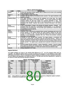
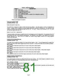
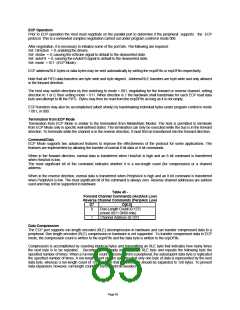
Table 43 - Mode Descriptions
DESCRIPTION*
SPP mode
PS/2 Parallel Port mode
Parallel Port Data FIFO mode
ECP Parallel Port mode
EPP mode (If this option is enabled in the configuration registers)
Reserved
Test mode
Configuration mode
MODE
000
001
010
011
100
101
110
111
*Refer to ECR Register Description
DATA and ecpAFifo PORT
ADDRESS OFFSET = 00H
Modes 000 and 001 (Data Port)
The Data Port is located at an offset of '00H' from the base address. The data register is cleared at initialization by
RESET. During a WRITE operation, the Data Register latches the contents of the data bus. The contents of this
register are buffered (non inverting) and output onto the PD0 - PD7 ports. During a READ operation, PD0 - PD7 ports
are read and output to the host CPU.
Mode 011 (ECP FIFO - Address/RLE)
A data byte written to this address is placed in the FIFO and tagged as an ECP Address/RLE. The hardware at the ECP
port transmits this byte to the peripheral automatically. The operation of this register is only defined for the forward
direction (direction is 0). Refer to the ECP Parallel Port Forward Timing Diagram, located in the Timing Diagrams
section of this data sheet.
DEVICE STATUS REGISTER (dsr)
ADDRESS OFFSET = 01H
The Status Port is located at an offset of '01H' from the base address. Bits 0 - 2 are not implemented as register bits,
during a read of the Printer Status Register these bits are a low level. The bits of the Status Port are defined as follows:
BIT 3 nFault
The level on the nFault input is read by the CPU as bit 3 of the Device Status Register.
BIT 4 Select
The level on the Select input is read by the CPU as bit 4 of the Device Status Register.
BIT 5 PError
The level on the PError input is read by the CPU as bit 5 of the Device Status Register. Printer Status Register.
BIT 6 nAck
The level on the nAck input is read by the CPU as bit 6 of the Device Status Register.
BIT 7 nBusy
The complement of the level on the BUSY input is read by the CPU as bit 7 of the Device Status Register.
DEVICE CONTROL REGISTER (dcr)
ADDRESS OFFSET = 02H
The Control Register is located at an offset of '02H' from the base address. The Control Register is initialized to zero by
the RESET input, bits 0 to 5 only being affected; bits 6 and 7 are hard wired low.
BIT 0 STROBE - STROBE
This bit is inverted and output onto the nSTROBE output.
BIT 1 AUTOFD - AUTOFEED
This bit is inverted and output onto the nAUTOFD output. A logic 1 causes the printer to generate a line feed after each
line is printed. A logic 0 means no autofeed.
BIT 2 nINIT - nINITIATE OUTPUT
This bit is output onto the nINIT output without inversion.
Page 81

 SMSC [ SMSC CORPORATION ]