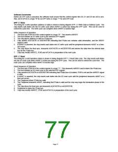
Software Constraints
Before an EPP cycle is executed, the software must ensure that the control register bits D0, D1 and D3 are set to zero.
Also, bit D5 (PCD) is a logic "0" for an EPP write or a logic "1" for and EPP read.
EPP 1.7 Write
The timing for a write operation (address or data) is shown in timing diagram EPP 1.7 Write Data or Address cycle. The
chip inserts wait states into the I/O write cycle when nWAIT is active low during the EPP cycle. This can be used to
extend the cycle time. The write cycle can complete when nWAIT is inactive high.
Write Sequence of Operation
1. The host sets PDIR bit in the control register to a logic "0". This asserts nWRITE.
2. The host initiates an I/O write cycle to the selected EPP register.
3. The chip places address or data on PData bus.
4. Chip asserts nDATASTB or nADDRSTRB indicating that PData bus contains valid information, and the WRITE
signal is valid.
5. If nWAIT is asserted, the chip inserts wait states into I/O write cycle until the peripheral deasserts nWAIT or a time-
out occurs.
6. The chip drives the final sync, deasserts nDATASTB or nADDRSTRB and latches the data from the internal data
bus for the PData bus.
7. Chip may modify nWRITE, PDIR and nPDATA in preparation of the next cycle.
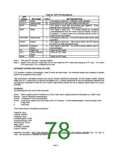
EPP 1.7 Read
The timing for a read operation (data) is shown in timing diagram EPP 1.7 Read Data cycle. The chip inserts wait states
into the I/O read cycle when nWAIT is active low during the EPP cycle. This can be used to extend the cycle time. The
read cycle can complete when nWAIT is inactive high.
Read Sequence of Operation
1. The host sets PDIR bit in the control register to a logic "1". This deasserts nWRITE and tri-states the PData bus.
2. The host initiates an I/O read cycle to the selected EPP register.
3. Chip asserts nDATASTB or nADDRSTRB indicating that PData bus is tri-stated, PDIR is set and the nWRITE signal
is valid.
4. If nWAIT is asserted, the chip inserts wait states into the I/O read cycle until the peripheral deasserts nWAIT or a
time-out occurs.
5. The Peripheral drives PData bus valid.
6. The Peripheral deasserts nWAIT, indicating that PData is valid and the chip may begin the termination phase of the
cycle.
7. The chip drives the final sync and deasserts nDATASTB or nADDRSTRB.
8. Peripheral tri-states the PData bus.
9. Chip may modify nWRITE, PDIR and nPDATA in preparation of the next cycle.
Page 77

 SMSC [ SMSC CORPORATION ]