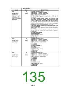
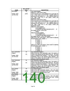
REG OFFSET
NAME
(hex)
41
DESCRIPTION
General Purpose I/0 bit 5.2
GP52
Bit[0] In/Out : =1 Input, =0 Output
Bit[1] Polarity : =1 Invert, =0 No Invert
Bit[3:2] Alternate Function Select
11=Reserved
Default = 0x01
on VTR POR
(R/W)
10=Reserved
01=RXD2
00=GPIO
Bits[6:4] Reserved
Bit[7] Output Type Select
1=Open Drain
0=Push Pull
GP53
42
General Purpose I/0 bit 5.3
Bit[0] In/Out : =1 Input, =0 Output
Bit[1] Polarity : =1 Invert, =0 No Invert
Bit[3:2] Alternate Function Select
11= Reserved
Default = 0x00
on VTR POR, VCC
POR and Hard
Reset
(R/W)
10= Reserved
(Note 4)
01=TXD2
00=GPIO
Bits[6:4] Reserved
Bit[7] Output Type Select
1=Open Drain
0=Push Pull
GP54
43
General Purpose I/0 bit 5.4
Bit[0] In/Out : =1 Input, =0 Output
Bit[1] Polarity : =1 Invert, =0 No Invert
Bit[3:2] Alternate Function Select
11= Reserved
Default = 0x01
on VTR POR
(R/W)
10= Reserved
01=nDSR2
00=GPIO
Bits[6:4] Reserved
Bit[7] Output Type Select
1=Open Drain
0=Push Pull
GP55
44
General Purpose I/0 bit 5.5
Bit[0] In/Out : =1 Input, =0 Output
Bit[1] Polarity : =1 Invert, =0 No Invert
Bit[3:2] Alternate Function Select
11= Reserved
Default = 0x01
on VTR POR
(R/W)
10= Reserved
01=nRTS2
00=GPIO
Bits[6:4] Reserved
Bit[7] Output Type Select
1=Open Drain
0=Push Pull
Page 136

 SMSC [ SMSC CORPORATION ]